XC9111A451ER 查看數據表(PDF) - TOREX SEMICONDUCTOR
零件编号
产品描述 (功能)
比赛名单
XC9111A451ER Datasheet PDF : 35 Pages
| |||
XC9110/XC9111 Series
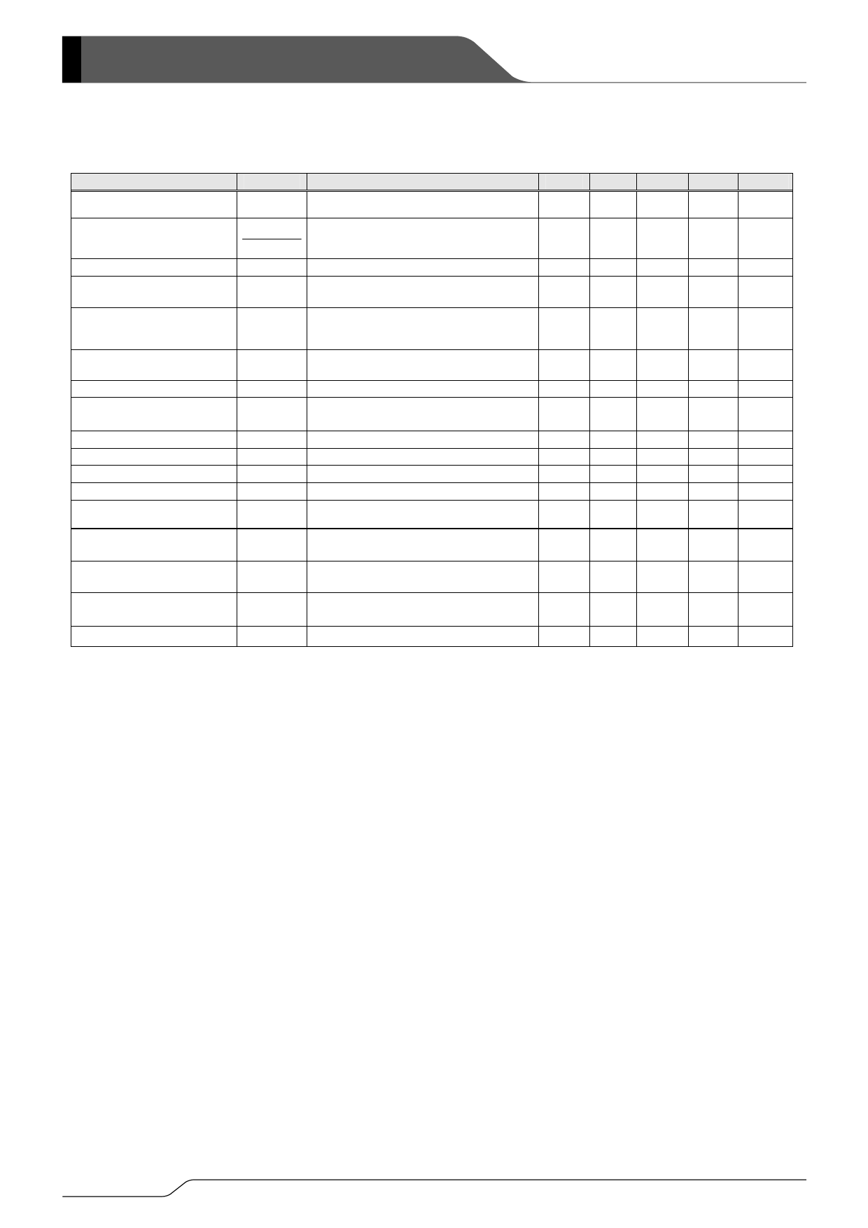
■ELECTRICAL CHARACTERISTICS
XC9111Axx1MR
PARAMETER
SYMBOL
Output Voltage
VOUT
Output Voltage Temperature
Characteristics
Maximum Input Voltage
△VOUT
△VOUT・△topr
VIN
Operating Start Voltage
VST1
CONDITIONS
Connected to external components
Connected to external components
- 40℃≦Topr≦85℃
IOUT=1mA,
Connected to external components
MIN.
×0.975
TYP. MAX.
VOUT ×1.025
Ta = 25℃
UNIT CIRCUIT
V
①
-
±100
-
ppm/
℃
①
10
-
-
V
①
-
0.8
0.9
V
①
Oscillation Start Voltage
VST2
Applied 0.8V to VOUT, Vpull=1.0V
-
-
0.8
V
②
Operating Hold Voltage
Input Current at No Load
VHLD
IIN
IOUT=1mA,
Connected to external components
IOUT=0mA (*1)
0.7
-
-
V
①
- E1-1(*) E1-2(*) μA
①
Supply Current 1 (*2)
IDD1
Applied (output voltage×0.95) to VOUT
- E2-1(*) E2-2(*) μA
②
Supply Current 2
IDD2
Applied (output voltage+0.5) to VOUT
- E3-1(*) E3-2(*) μA
②
Lx Switch ON Resistance RSWON
Same as IDD1, VLx=0.4V (*3)
- E4-1(*) E4-2(*) Ω
②
Lx Leak Current
ILxL
Same as IDD2, VLx=7V
-
-
1
μA
③
Duty Ratio
DTY
Same as IDD1, measure Lx waveform E7-1(*) E7-2(*) E7-3(*) %
②
Duty Ratio 2
DTY2
IOUT=1mA, measure Lx ON time.
Connect to external components
48
56
64
%
①
Maximum Oscillation
Frequency
MAXFOSC
Same as IDD1
85
100 115
kHz
②
Maximum Oscillation
Frequency 2
MAXFOSC2
Same as IDD1
153
180
207
kHz
②
Lx Limit Voltage (*4)
VLxLMT
Same as IDD1, VLx when max. oscillation
frequency is more than double
0.7
-
1.1
V
②
Efficiency (*5)
EFFI
Connect to external components
-
E8(*)
-
%
①
Test condition : Unless otherwise specified, VIN=VOUT×0.6, IOUT=<C1(*)>, Vpull=5.0V
NOTE:
*1: TOREX SBD, XB01SB04A2BR is used, reverse current IR < 1μA (when reverse voltage VR = 10V is applied), in case of using selected
parts.
*2: Supply Current 1 is the value when the IC is constantly switching. In actual operation, the oscillator periodically switches, resulting in
lower power consumption. Please refer to Input Current (IIN) under no load condition for the actual current, which is supplied from the
input power supply (VIN).
*3: Lx switch ON resistance can be calculated by (VLx x Rp) / (Vpull - VLx). * Change Vpull so that VLx will become 0.4V.
*4: The Lx limit voltage function becomes stable when VOUT is over 2.0V.
*5: EFFI={[output voltage]×(output current)} / [(input voltage)×(input current)]×100
*6: Please be aware of the absolute maximum ratings of the external components.
(*): Please refer to the charts.
6/35
Share Link: 