LC8905V 查看數據表(PDF) - SANYO -> Panasonic
零件编号
产品描述 (功能)
比赛名单
LC8905V Datasheet PDF : 16 Pages
| |||
LC8905V
Functions
1. Data Input and Output (DIN1, DIN2, E/DOUT)
The DIN1 pin has a built-in amplifier, and can receive signals with an amplitude of about 400 mVp-p (coaxial input).
The DIN2 pin is only for use with optical modules.
Note that although the data input pins are controlled by the microprocessor, DIN1 can be selected when a
microprocessor is not used. The microprocessor interface pins must be tied low in such applications.
The E/DOUT normally outputs channel status information. However, it can be set to output either the input bi-phase
data or the validity flag by command codes from the microprocessor.
2. PLL (R, VIN, VCO, AVOCK)
This circuit includes a built-in VCO and supports sampling frequencies of 32, 44.1, and 48 kHz.
The resistor connected to R functions as both the VCO gain control and as temperature compensation. The VIN pin
sets the VCO free-running frequency.
The PLL circuit can be reset within a fixed period when it operates incorrectly, for example, if a lock pull-in failure
occurs, by inputting an asynchronous, continuously operating clock signal to the AVOCK pin.
3. Clock Settings and Output (FS128, BCK, LRCK, DATAOUT, CKSEL, CKOUT)
A 128fs clock signal is output from the FS128 pin. Figure 1 shows the output timing for the BCK, LRCK, and
DATAOUT pins.
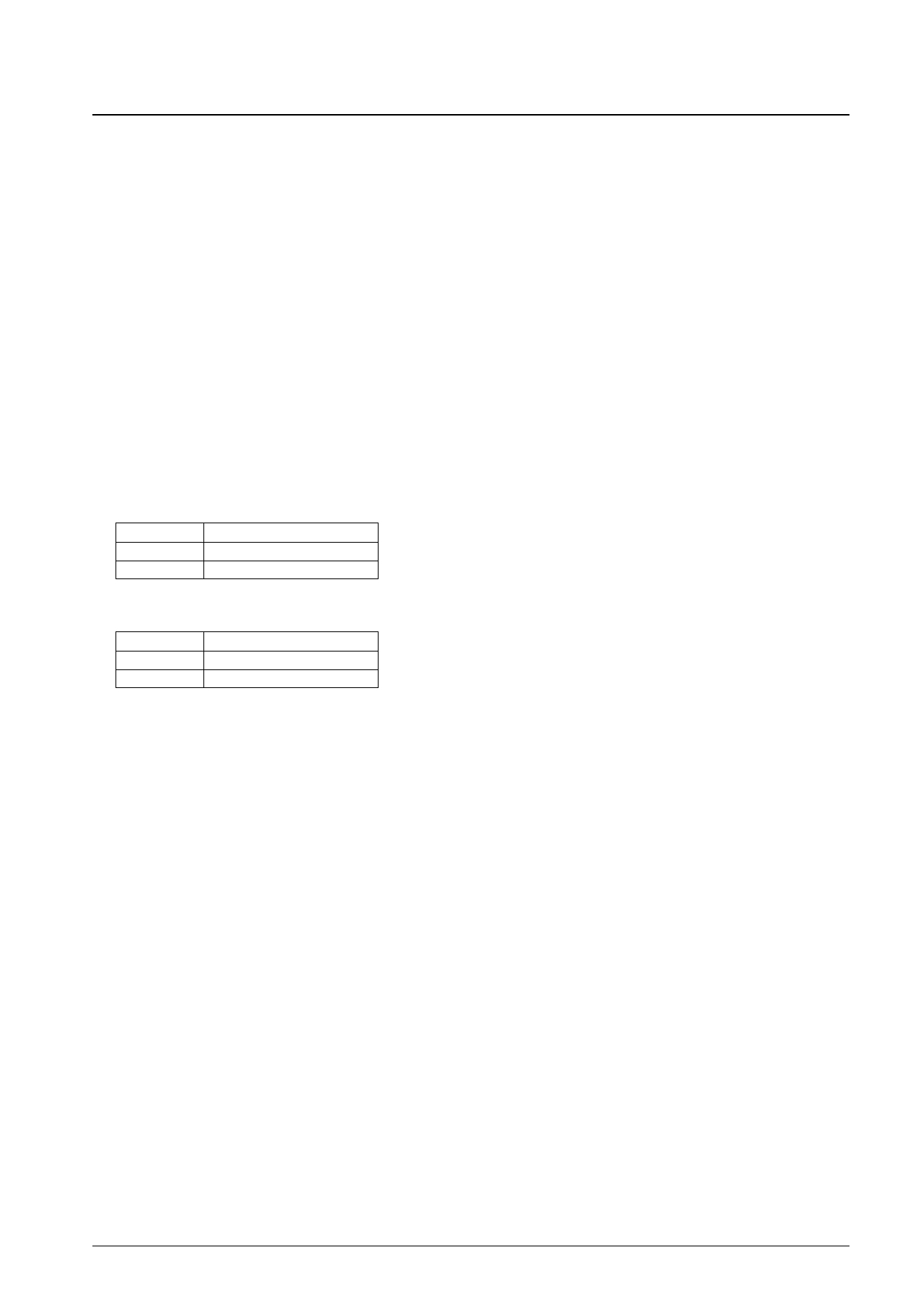
The CKOUT clock output is set by the CKSEL pin as listed in the table below.
CKSEL
L
H
CKOUT
384fs clock output
512fs clock output
The microprocessor interface format is also set by CKSEL as listed in the table below.
CKSEL
L
H
Microprocessor interface
Figure 2
Figure 3
No. 5237-8/16
Share Link: 