LM7001J 查看數據表(PDF) - SANYO -> Panasonic
零件编号
产品描述 (功能)
比赛名单
LM7001J Datasheet PDF : 8 Pages
| |||
LM7001J, 7001JM
(4) R0 to R2: Reference frequency data
R0
R1
R2
fref [kHz] BO1
BO2
BO3
0
0
0
100
1
1
0
0
0
1
50
1
1
0
0
1
0
25
1
1
0
0
1
1
5
0
0
1
1
0
0
10
1
0
1
1
0
1
9
1
0
1
1
1
0
1
0
1
1
1
1
1
5
0
0
1
Note: The values listed for BO1, BO2, and BO3 are for the case when the B0 to B2 data is set to all zeros.
(5) S: Divider selection data
1: FMIN, 0: AMIN
Notes on PLL IC Usage
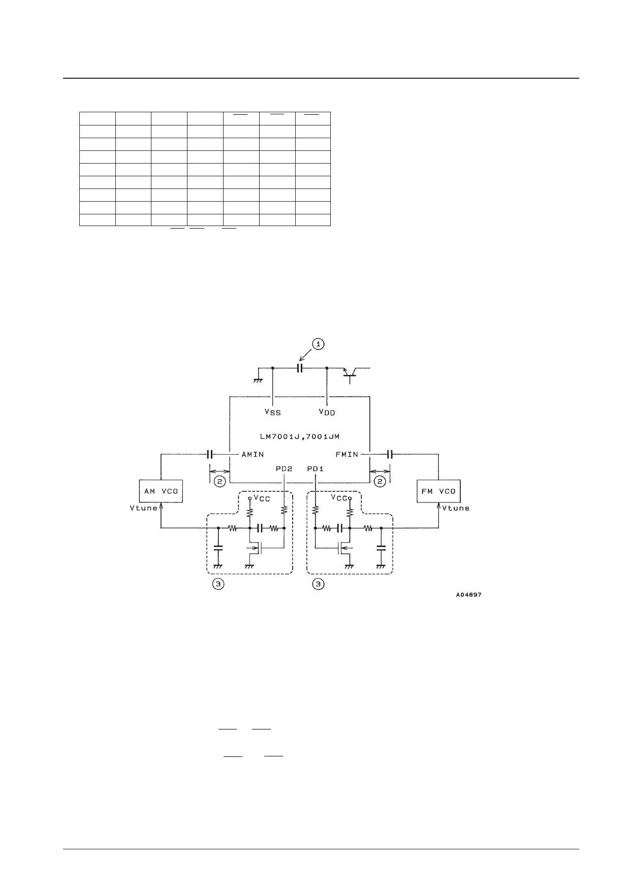
1. PLL IC printed circuit board patterns
x Power supply pins
A capacitor must be inserted between the VDD and VSS power supply pins for noise exclusion. This capacitor
must be located as close as possible to these pins.
y FMIN and AMIN pins
The coupling capacitors must be located as close as possible to these pins.
z PD pins, low-pass filter
Since those are high-impedance pins, they are susceptible to noise. Therefore, the pattern should be kept as short
as possible and the area around this circuit should be covered by the ground pattern.
2. Initial states of the output ports (BO1 to BO3)
The initial states of the output ports after power is applied are undefined until data has been transferred.
In particular, it is possible for the BO1 and BO3 pins to output the internal clock, so data must be transferred as soon
as possible.
However, note that the LSI cannot accept data until the crystal oscillator is operating normally.
No. 5262-7/8
Share Link: 