IMIZ9972BA 查看數據表(PDF) - Cypress Semiconductor
零件编号
产品描述 (功能)
比赛名单
IMIZ9972BA Datasheet PDF : 9 Pages
| |||
Z9972
Maximum Ratings[4]
Maximum Input Voltage Relative to VSS: ............ VSS – 0.3V
Maximum Input Voltage Relative to VDD: ............. VDD + 0.3V
Storage Temperature: ................................–65°C to + 150°C
Operating Temperature: ................................ –40°C to +85°C
Maximum ESD protection ............................................... 2 kV
Maximum Power Supply: ................................................5.5V
Maximum Input Current: ............................................±20 mA
This device contains circuitry to protect the inputs against
damage due to high static voltages or electric field; however,
precautions should be taken to avoid application of any
voltage higher than the maximum rated voltages to this circuit.
For proper operation, VIN and VOUT should be constrained to
the range:
VSS < (VIN or VOUT) < VDD.
Unused inputs must always be tied to an appropriate logic
voltage level (either VSS or VDD).
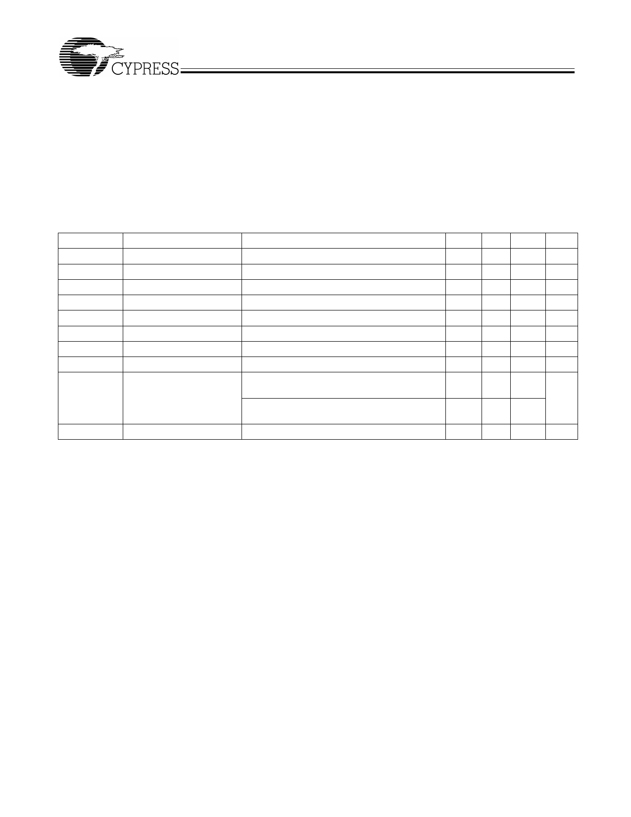
DC Parameters VDD = 2.9V to 3.6V, VDDC = 3.3V ±10%, TA = –40°C to +85°C
Parameters
Description
Conditions
Min. Typ.
VIL
Input LOW Voltage
VSS
VIH
Input HIGH Voltage
2.0
IIL
Input LOW Current[5]
IIH
Input HIGH Current
VOL
Output LOW Voltage[6]
IOL = 20 mA
VOH
Output HIGH Voltage[6]
IOH = –20 mA
2.4
IDDQ
Quiescent Supply Current
10
IDDA
PLL Supply Current
VDD only
15
IDD
Dynamic Supply Current QA and QB @ 60 MHz
225
QC @ 120 MHz, CL = 30pF
QA and QB @ 25 MHz
125
QC @ 50 MHz, CL = 30pF
CIN
Input Pin Capacitance
4
Notes:
4. The voltage on any input or I/O pin cannot exceed the power pin during power-up. Power supply sequencing is NOT required.
5. Inputs have pull-up/pull-down resistors that effect input current.
6. Driving series or parallel terminated 50Ω (or 50Ω to VDD/2) transmission lines.
Max.
0.8
VDD
–120
10
0.5
15
20
Unit
V
V
µA
µA
V
V
mA
mA
mA
pF
Document #: 38-07088 Rev. *D
Page 6 of 9
Share Link: 