LC75712E 查看數據表(PDF) - SANYO -> Panasonic
零件编号
产品描述 (功能)
比赛名单
LC75712E Datasheet PDF : 21 Pages
| |||
LC75710NE, 75711NE, 75712E
Detailed Instruction Descriptions
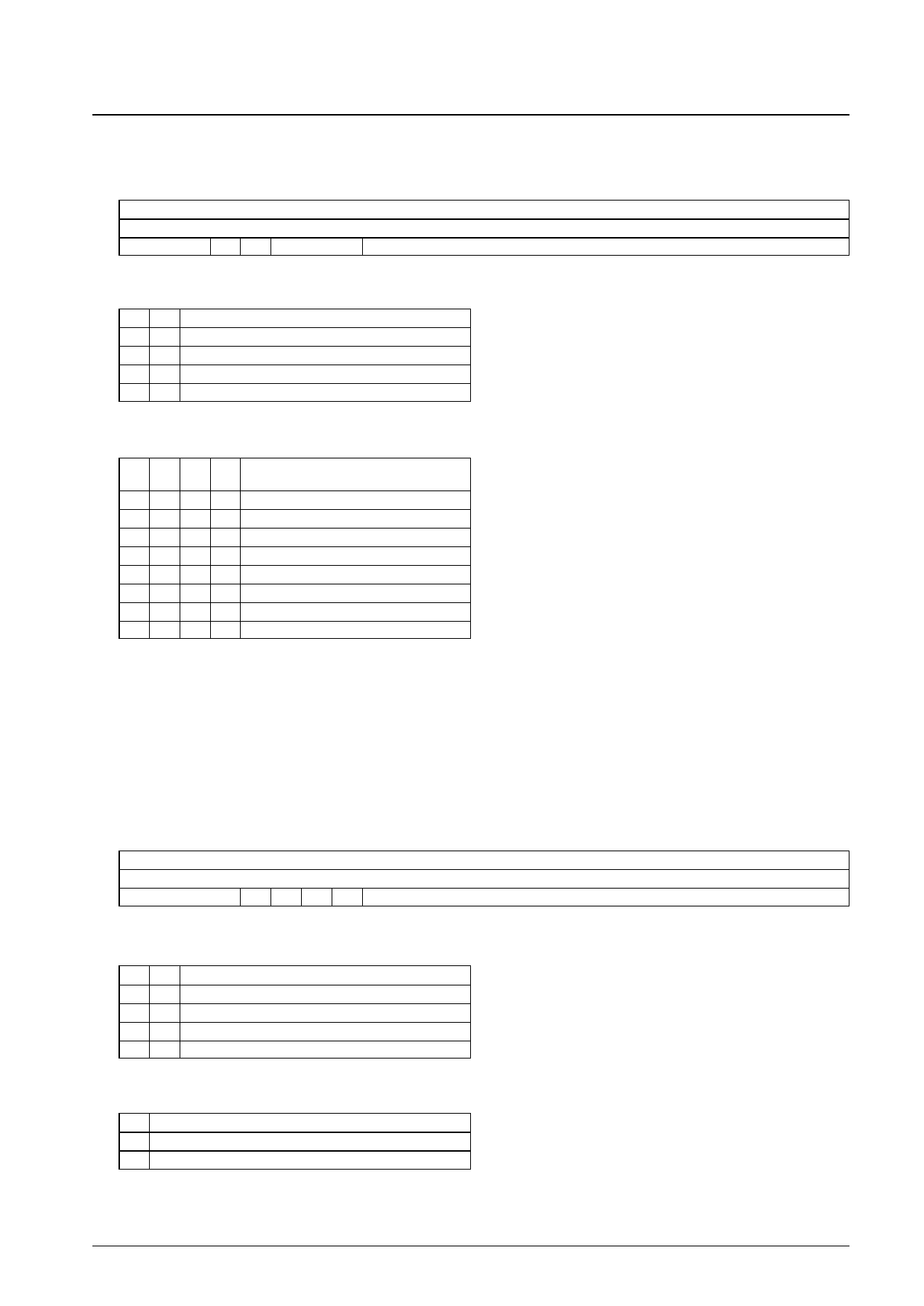
1. Display blink........................................<Blinks the display.>
Code
D23 D22 D21 D20 D19 D18 D17 D16 D15 D14 D13 D12 D11 D10 D9 D8 D7 D6 D5 D4 D3 D2 D1 D0
1 0 1 M A BC2 BC1 BC0 G16 G15 G14 G13 G12 G11 G10 G9 G8 G7 G6 G5 G4 G3 G2 G1
M, A: Data that specifies the blinking operation
MA
Display operating state
0 0 Neither MDATA nor ADATA blinks.
0 1 Only ADATA blinks.
1 0 Only MDATA blinks.
1 1 Both ADATA and MDATA blink.
BC0 to BC2: Blink period setting
BC2 BC1 BC0 HEX
Blink Period (s)*1
(when fOSC is 2.7 MHz)
0 0 0 0 Blink operation is stopped.
0 0 1 1 0.1
0 1 0 2 0.2
0 1 1 3 0.3
1 0 0 4 0.4
1 0 1 5 0.5
1 1 0 6 0.8
1 1 1 7 1.0
G1 to G16: Blinking digit specification
Each bit Gn (where n is an integer between 1 and 16) specifies that blinking be applied to grid output pin Gn when
the corresponding bit Gn is 1.
This instruction is used to specify the blinking operation. Not only can an arbitrary digit be specified, but MDATA
and ADATA can also be specified. There are also seven blinking periods.
Note: 1. When the blinking period needs to be controlled precisely the display should be blinked by repeatedly
turning the display on and off using the display on/off control instruction.
2. Display on/off control ..........................<Turns the display on or off.>
Code
D23 D22 D21 D20 D19 D18 D17 D16 D15 D14 D13 D12 D11 D10 D9 D8 D7 D6 D5 D4 D3 D2 D1 D0
0 0 0 1 * M A O G16 G15 G14 G13 G12 G11 G10 G9 G8 G7 G6 G5 G4 G3 G2 G1
*: Don’t care.
M, A: Specifies the data to be turned on or off.
MA
Display operating state
0 0 Both MDATA and ADATA turn off.
0 1 Only ADATA turns on.
1 0 Only MDATA turns on.
1 1 Both ADATA and MDATA turn on.
O: On/off control
O
0 Off
1 On
Display state
When the display is turned off with an O value of 0, the data can be displayed immediately with an O value of 1
since the display data remains in DCRAM.
No. 4907-10/21
Share Link: 