LC75711NE 查看數據表(PDF) - SANYO -> Panasonic
零件编号
产品描述 (功能)
比赛名单
LC75711NE Datasheet PDF : 21 Pages
| |||
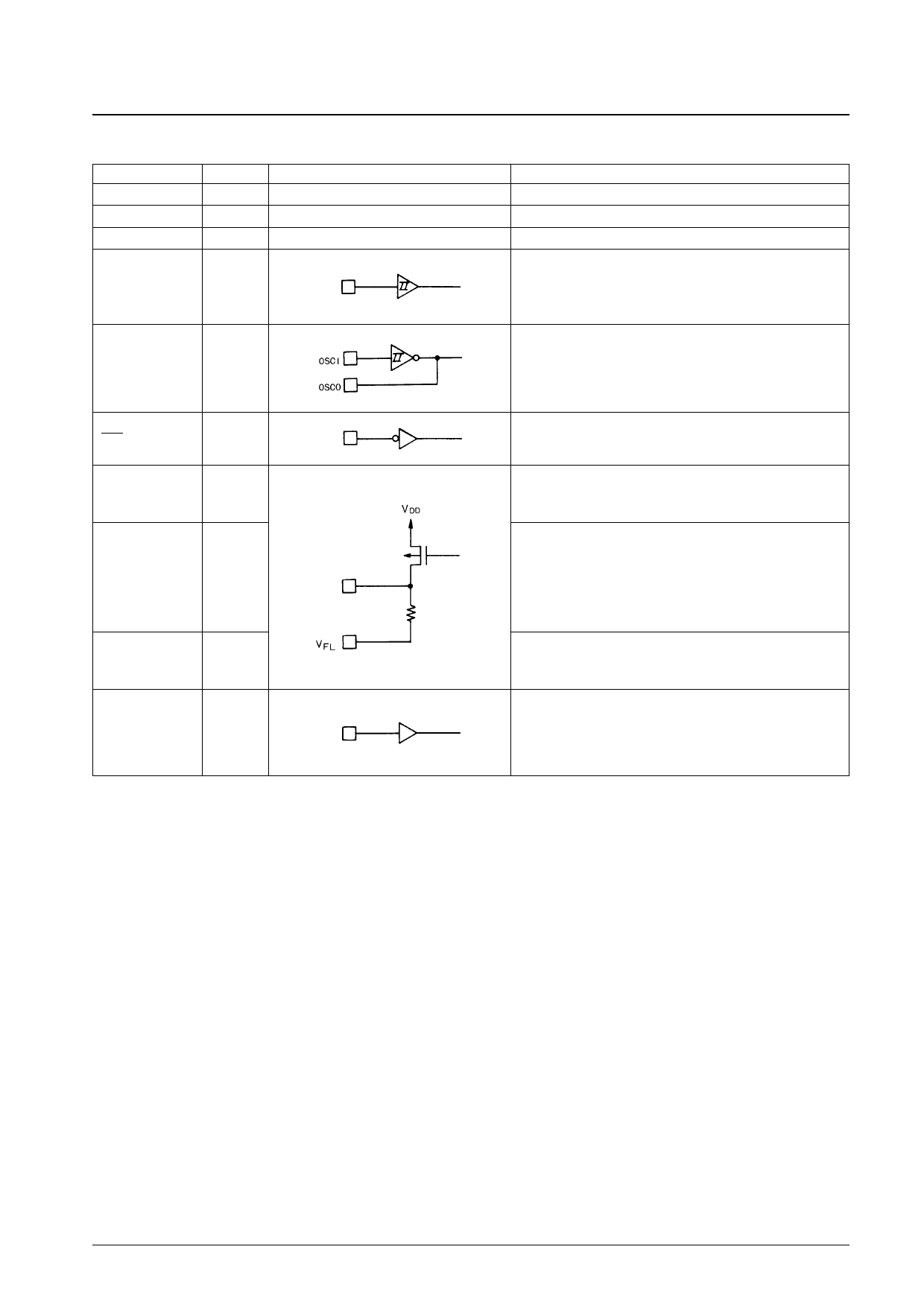
Pin Functions
Pin
No.
VDD
1
VSS
1
VFL
1
DI
1
CL
1
CE
1
OSCI
1
OSCO
1
RES
1
AM1 to AM35
AA1 to AA3
38
AA4/G16
AA5/G15
AA6/G14
5
AA7/G13
AA8/G12
G1 to G11
11
TEST
1
LC75710NE, 75711NE, 75712E
Pin circuit
Function
Logic block power supply: +5 V (typical)
Logic block power supply: ground
Driver block power supply
Serial data interface
DI: Transfer data
CL: Synchronization clock
CE: Chip enable
External oscillator RC circuit connections
System reset input
Anode outputs
Pull-down resistors are built in.
Anode/grid outputs
These pins function as grid output pins when the number of
displayed digits is selected to be between 12 and 16 digits with
the “Grid register load” instruction.
Pull-down resistors are built in.
Grid outputs
Pull-down resistors are built in.
LSI testing
This pin must be connected to VSS during normal operation.
No. 4907-5/21
Share Link: 