MC74F253D 查看數據表(PDF) - Motorola => Freescale
零件编号
产品描述 (功能)
比赛名单
MC74F253D Datasheet PDF : 3 Pages
| |||
MC54/74F253
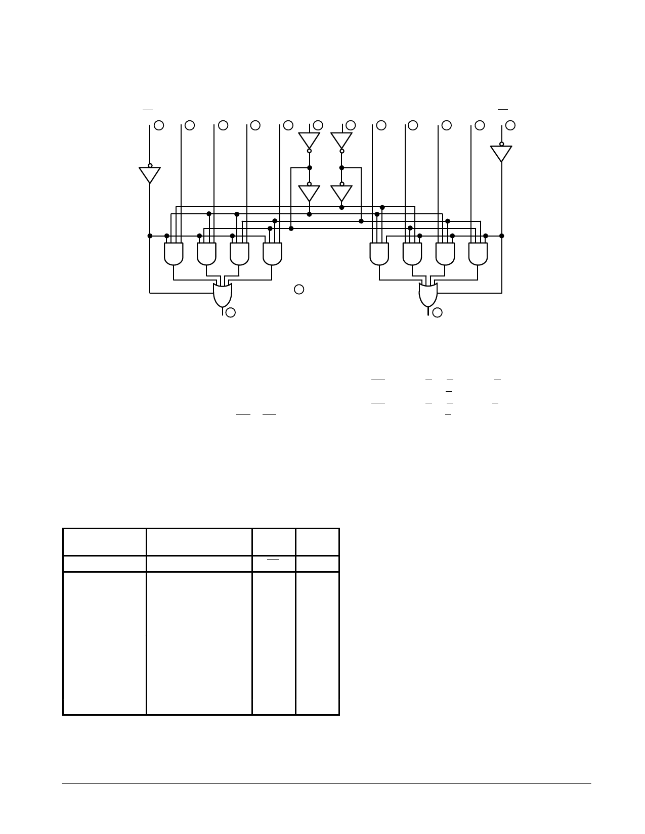
LOGIC DIAGRAM
OEb 13b
12b
11b
10b S0
S1
13a
12a
11a
10a OEa
15
13
12
11
10
14
2
3
4
5
6
1
Zb 9
VCC = PIN 16
GND = PIN 8
= PIN NUMBERS
Za 7
FUNCTIONAL DESCRIPTION
The F253 contains two identical 4-input Multiplexers with
3-State Outputs. They select two bits from four sources se-
lected by common Select Inputs (S0, S1). The 4-input multi-
plexers have individual Output Enable (OEa, OEb) inputs
which, when HIGH, force the outputs to a high impedance
(high Z) state.
The F253 is the logic implementation of a 2-pole, 4-position
switch, where the position of the switch is determined by the
logic levels supplied to the two select inputs. The logic equa-
tions for the outputs are shown below:
Za = OEa • (I0a • S1 • S0 + I1a • S1 • S0 +
I2a • S1 • S0 + 13a • S1 • S0)
Zb = OEb • (I0b • S1 • S0 + I1b • S1 • S0 +
I2b • S1 • S0 + I3b • S1 • S0)
If the outputs of 3-state devices are tied together, all but one
device must be in the high impedance state to avoid high cur-
rents that would exceed the maximum ratings. Designers
should ensure that Output Enable signals to 3-state devices
whose outputs are tied together are designed so that there is
no overlap.
FUNCTION TABLE
Select
Inputs
Data Inputs
S0
S1
I0 I1 I2 I3
X
X
XXXX
L
L
LXXX
L
L
HXXX
H
L
XLXX
H
L
XHXX
L
H
XXLX
L
H
XXHX
H
H
XXXL
H
H
XXXH
Output
Enable
OE
H
L
L
L
L
L
L
L
L
Output
Z
Z
L
H
L
H
L
H
L
H
H = HIGH Voltage Level
L = LOW Voltage Level
X = Don’t Care
Z = High Impedance (off)
Address inputs S0 and S1
are common to both sections.
FAST AND LS TTL DATA
4-121
Share Link: 