100301QC 查看數據表(PDF) - Fairchild Semiconductor
零件编号
产品描述 (功能)
比赛名单
100301QC Datasheet PDF : 7 Pages
| |||
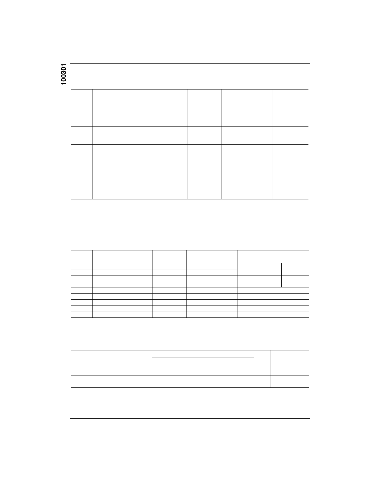
Commercial Version (Continued)
SOIC and PLCC AC Electrical Characteristics
VEE = −4.2V to −5.7V, VCC = VCCA = GND
Symbol
Parameter
TC = 0°C
Min
Max
TC = +25°C
Min
Max
TC = +85°C
Min
Max
Units
Conditions
tPLH
tPHL
tTLH
tTHL
tOSHL
Propagation Delay
Data to Output
Transition Time
20% to 80%, 80% to 20%
Maximum Skew Common Edge
Output-to-Output Variation
0.50
1.00
0.50
1.05
0.50
1.10
0.40
1.10
0.40
1.10
0.40
1.10
240
240
240
Figures 1, 2
ns
(Note 5)
ns Figures 1, 2
PLCC Only
ps (Note 6)
Data to Output Path
tOSLH
Maximum Skew Common Edge
Output-to-Output Variation
PLCC Only
330
330
330
ps (Note 6)
Data to Output Path
tOST
Maximum Skew Opposite Edge
Output-to-Output Variation
PLCC Only
330
330
330
ps (Note 6)
Data to Output Path
tPS
Maximum Skew
Pin (Signal) Transition Variation
PLCC Only
230
230
230
ps (Note 6)
Data to Output Path
Note 5: The propagation delay specified is for single output switching. Delays may vary up to 100 ps with multiple outputs switching.
Note 6: Output-to-Output Skew is defined as the absolute value of the difference between the actual propagation delay for any outputs within the same pack-
aged device. The specifications apply to any outputs switching in the same direction either HIGH-to-LOW (tOSHL), or LOW-to-HIGH (tOSLH), or in opposite
directions both HL and LH (tOST). Parameters tOST and tPS guaranteed by design.
Industrial Version
PLCC DC Electrical Characteristics (Note 7)
VEE = −4.2V to −5.7V, VCC = VCCA = GND, TC = −40°C to +85°C
Symbol
Parameter
TC = −40°C
Min
Max
TC = 0°C to +85°C
Min
Max
Units
Conditions
VOH
Output HIGH Voltage
−1085 −870 −1025 −870
mV VIN = VIH(Max)
Loading with
VOL
Output LOW Voltage
−1830 −1575 −1830 −1620
mV or VIL(Min)
50Ω to −2.0V
VOHC
Output HIGH Voltage
−1095
−1035
mV VIN = VIH(Min)
Loading with
VOLC
Output LOW Voltage
−1565
−1610
mV or VIL(Max)
50Ω to −2.0V
VIH
Input HIGH Voltage
−1170 −870 −1165 −870
mV Guaranteed HIGH Signal for All Inputs
VIL
Input LOW Voltage
−1830 −1480 −1830 −1475 mV Guaranteed LOW Signal for All Inputs
IIL
Input LOW Current
0.50
0.50
µA
VIN = VIL(Min)
IIH
Input HIGH Current
240
240
µA
VIN = VIH(Max)
IEE
Power Supply Current
−29
−15
−29
−15
mA Inputs Open
Note 7: The specified limits represent the “worst case” value for the parameter. Since these values normally occur at the temperature extremes, additional
noise immunity and guardbanding can be achieved by decreasing the allowable system operating ranges. Conditions for testing shown in the tables are cho-
sen to guarantee operation under “worst case” conditions.
PLCC AC Electrical Characteristics
VEE = −4.2V to −5.7V, VCC = VCCA = GND
Symbol
Parameter
TC = −40°C
Min
Max
TC = +25°C
Min
Max
TC = +85°C
Min
Max
Units
tPLH
Propagation Delay
tPHL
Data to Output
0.40
1.00
0.50
1.05
0.50
1.10
ns
tTLH
Transition Time
tTHL
20% to 80%, 80% to 20%
0.30
1.10
0.40
1.10
0.40
1.10
ns
Note 8: The propagation delay specified is for single output switching. Delays may vary up to 100 ps with multiple outputs switching.
Conditions
Figures 1, 2
(Note 8)
Figures 1, 2
www.fairchildsemi.com
4
Share Link: 