AD74322AAR 查看數據表(PDF) - Analog Devices
零件编号
产品描述 (功能)
比赛名单
AD74322AAR Datasheet PDF : 20 Pages
| |||
PRELIMINARY TECHNICAL DATA
AD74322
INTERFACING
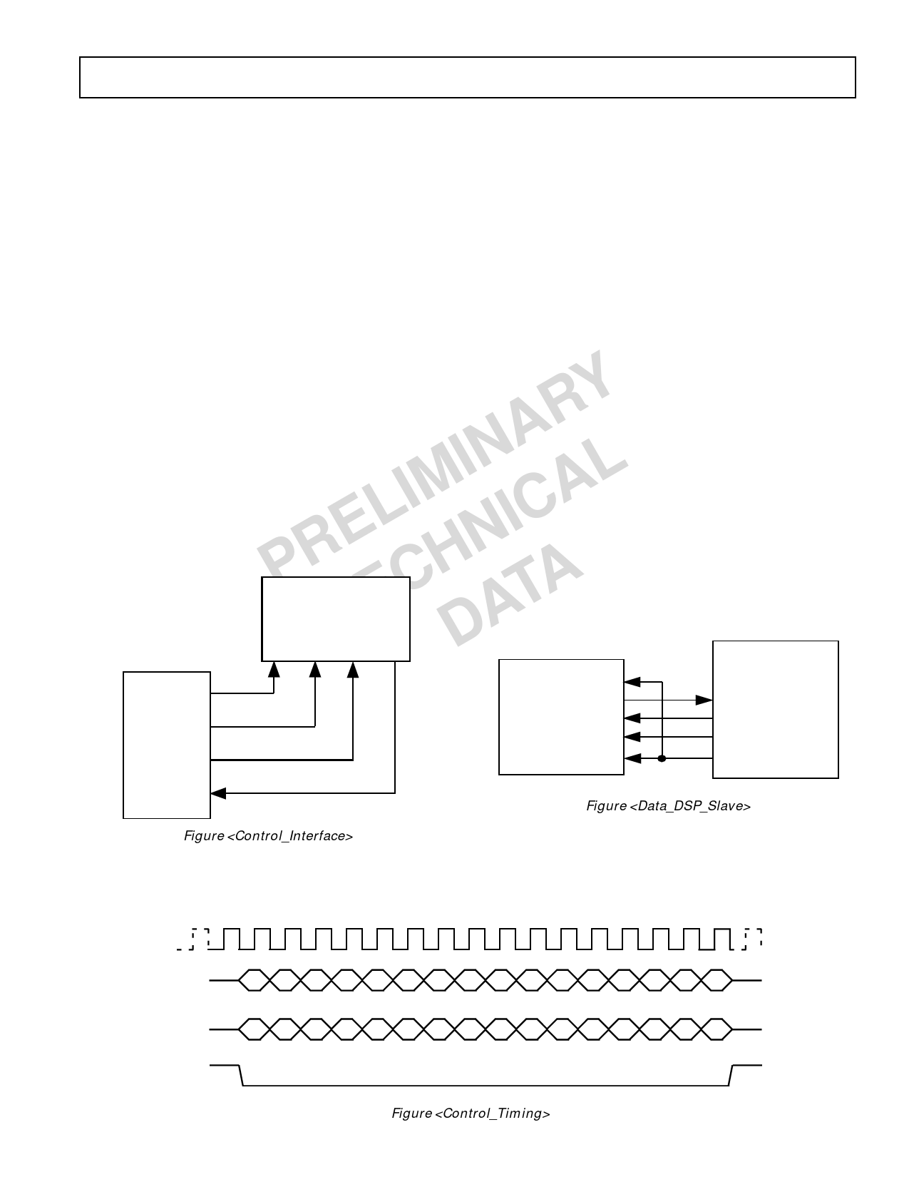
Data in and out of the Control Port go through a 16-bit
TheAD74322featurestwoseparateinterfaces,ControlandData,which shift register whose contents are mapped to the internal
are used to program control settings and send/receive sample data
registers using the mapping scheme of Figure
respectively. The Control interface is implemented using an SPI type
<ContPortMap>. A 16-bit word received by the Control
protocolbuttransfers16-bitsperframe.TheDatainterfaceuseseithera Port is decoded as a read or write to a register address set
DSPor I2Sprotocoltotransferstereodatasamplesbetweencontroller by bits 15 - 12. This 4-bit register address selects 1 of 16
andcodec.TheDSPcompatibleinterfacemodeallowsdatasamplestobe registers as shown in Table <ContRegMap>. Bit 11
transferredinaprotocolthatissupportedbytheserialinterfacesofmost selects whether a register read or write is requested -
fixed- and floating-point DSPs.
Write = 0, Read = 1. Bit-10 is reserved. Bits 9 through 0
In order to reduce peripheral requirements when interfacing the AD74322
with the host DSP, the DSP mode allows the DSP to send both data and
contain register data. Each Control register’s contents are
detailed below.
controlinformationtothedeviceviathedatainterface.Thisisthedefault DataInterface
modeandrequiresuserstoonlyuseasingleDSPSPORTtobothcontrol Therearetwomodesofoperationofthedatainterface:DSPmodeand
the device and service it with data samples.
I2S mode. The default mode of the data interface is a DSP mode which
Control Interface
combines control and data functions in a single protocol. This is to reduce
Control of the AD74322 operation is via a set of 16 Control Registers
which are programmed through the Control Port. The Control Port
Y protocol is similar to the SPIÒ protocol with the exception that 16-bits of
R data are transferred per frame. The Control Port consists of the following
pins: CCLK - Control Port Serial Clock, CLATCH - Control Port Latch
A or Frame signal, CDIN - Control Port Serial Data In and CDOUT -
IN Control Port Data Out. CLATCH is a framing signal that is active low.
L When asserted, it gates the other interface lines as being active. CCLK is
IM A usedtoclockinputdataonCDINandclockoutput(readback)dataon
L IC CDOUT.Figure<Control_Interface>detailstheconnectivityofthe
Control Port to a controller and Figure <Control_Timing> details the
E N interfacetiming.
PRTECHDATA AD743xx
the peripheral overhead required on the DSP when interfacing to the
AD74322. This mode operates in a standard DSP serial format. In I2S
mode the data interface streams audio data samples being sent to or
received from the DACs and ADCs respectively, using the I2S serial
protocol.
In either mode it can be configured as either a master or slave device
ensuring connectivity to the largest number of host processors.
DSP Mode
The DSP mode allows interfacing to most fixed- and floating-point DSPs
as well as other processors such as RISCs etc that having serial ports that
support synchronous communications. The key feature of synchronous
DSP communications is that the serial data is framed by a separate Frame
Sync signal. Figures <Data_DSP_Slave> and <Data_DSP_Master> detail
connectivity in Master Mode (codec is master) and Slave Mode (codec is
slave) respectively.
CDIN CLATCH CCLK CDOUT
AD743xx
(MASTER)
TFS
LRCLK/SDIFS
CONTROLLER
DSP
(SLAVE)
DT
SCLK
DR
RFS
DSDATA/SDI
BCLK/SCLK
ASDATA/SDO
SDOFS
Figure <Control_Interface>
Figure <Data_DSP_Slave>
CCLK
CDIN
MSB 14 13 12 11 10
9
8
7
6
5
4
3
2
1 LSB
CDOUT
MSB 14 13 12 11 10
9
8
7
6
5
4
3
2
1 LSB
CLATCH
Pr D 03/00
Figure <Control_Timing>
–11–
Share Link: 