TDA7580 查看數據表(PDF) - STMicroelectronics
零件编号
产品描述 (功能)
比赛名单
TDA7580 Datasheet PDF : 39 Pages
| |||
TDA7580
Block diagram and electrical specifications
2
Block diagram and electrical specifications
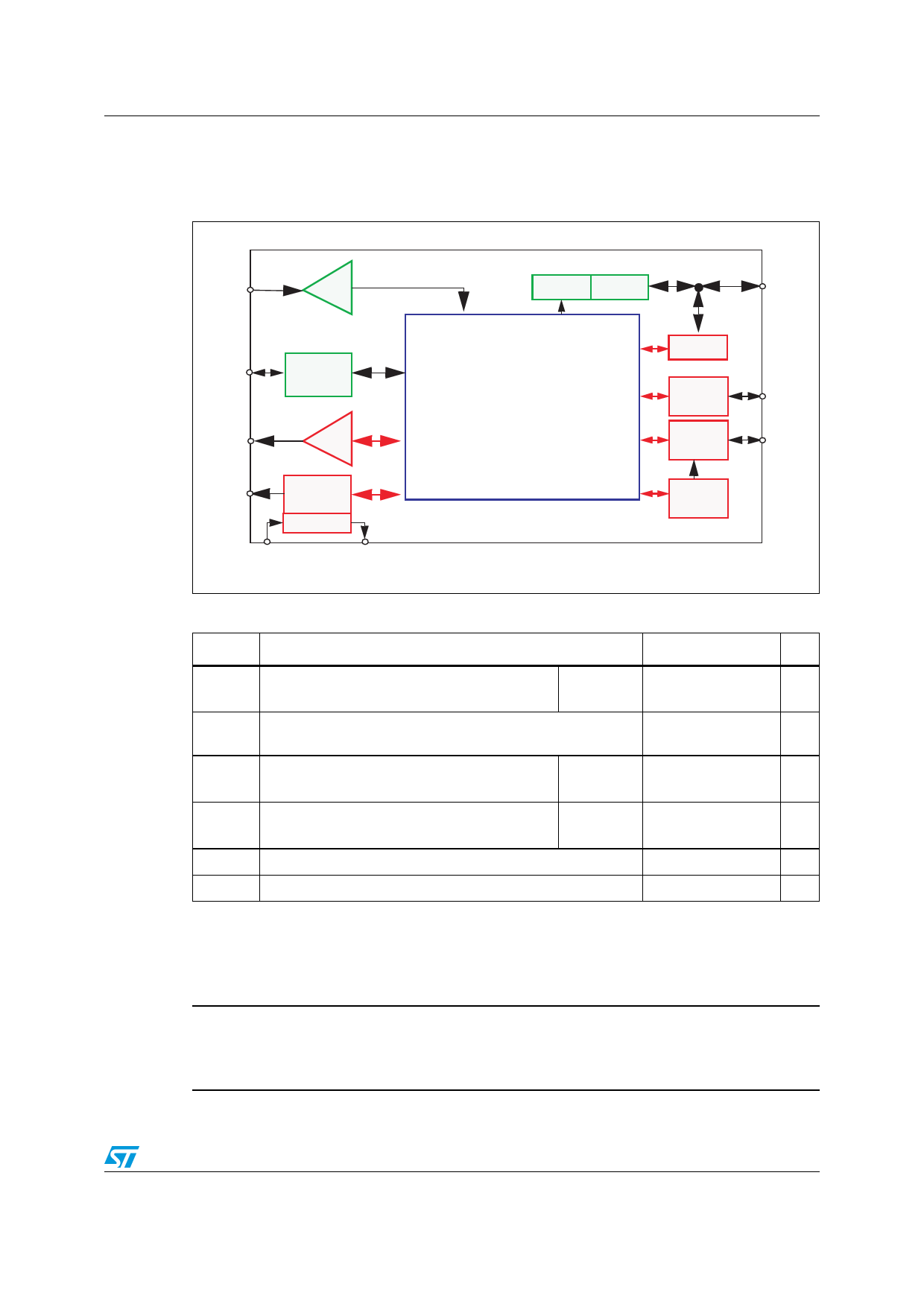
Figure 1. Block diagram
A/D
HS3I
DAC
CGU
Oscillator
RDS
I2C/SPI
IF digital
Signal processor
I2C/SPI
SAI1
SAI0
SRC
Table 2. Absolute maximum ratings
Symbol
Parameter
Value
Unit
VDD
VDD3
Power supplies (1)
Nom. 1.8V
-0.5 to 2.5
V
Nom. 3.3V
-0.5 to 4.0
V
Analog input or output voltage belonging to 3.3V IO ring
(VDDSD, VDDOSC)
-0.5 to 4.0
V
Digital input or output voltage, 5V tolerant
Normal(2)
Failsafe(3)
-0.5 to 6.50
-0.5 to 3.80
V
V
All remaining digital input or output voltage
Nom. 1.8V -0.5 to (VDD+0.5)
V
Nom. 3.3V -0.5 to (VDD3+0.5)
Tj Operating junction temperature range
-40 to 125
°C
Tstg Storage temperature
-55 to 150
°C
1. VDD3 refers to all of the nominal 3.3V power supplies (VDDH, VOSC, VDDSD). VDD refers to all of the nominal
1.8V power supplies (VDD, VMTR).
2. During Normal Mode operation VDD3 is always available as specified.
3. During Fail-safe Mode operation VDD3 may be not available.
Warning: Operation at or beyond these limits may result in permanent
damage to the device. Normal operation is not guaranteed at
these extremes.
7/39
Share Link: 