FX631 查看數據表(PDF) - CML Microsystems Plc
零件编号
产品描述 (功能)
比赛名单
FX631 Datasheet PDF : 8 Pages
| |||
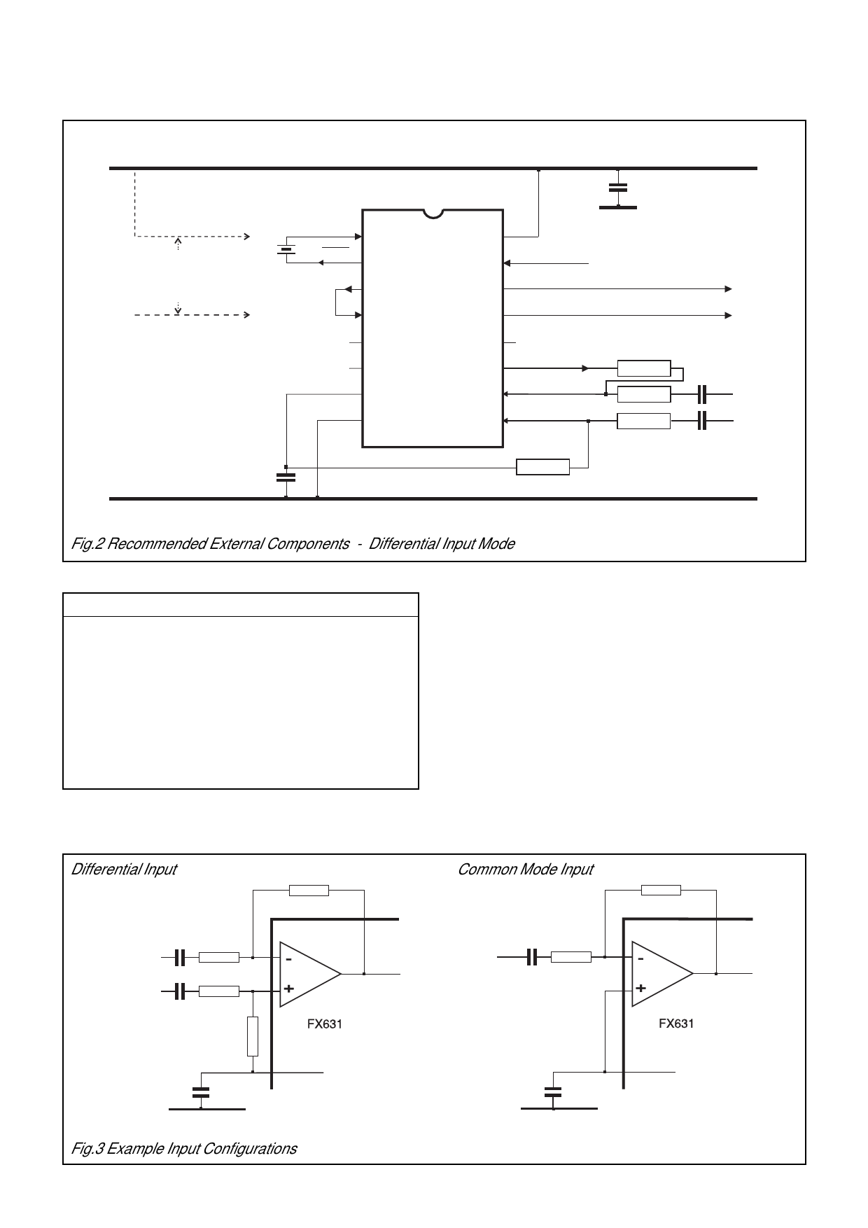
Application Information
External Components
VDD
C1
XTAL/CLOCK
XTAL/CLOCK
X1
1
For use with a Clock Pulse input
- Remove Xtal (X1)
XTAL
2
- Connect Pin 1 to VDD
- Remove link (Pins 3/4)
- Input clock pulses to CLOCK IN
CLOCK OUT
3
VSS
16
VDD
SYSTEM
15
PACKET MODE OUTPUT
14
CLOCK IN
CLOCK IN
TONE FOLLOWER OUTPUT
4
13
FX631DW
5
6
VBIAS
7
VSS 8
12
AMP OUT
11
SIGNAL IN (-)
10
SIGNAL IN (+)
9
R4
R1
C3
R2
R3
C4
C2
VSS
Fig.2 Recommended External Components - Differential Input Mode
Component
R1
R2
R3
R4
C1
C
2
C
3
C4
X1
Value
RFEEDBACK
RIN (-)
RIN (+)
RBIAS
1.0µF ±20%
1.0µF ±20%
C
IN (-)
CIN (+)
3.579545MHz
External Components
1. The values of the Input Amp gain components
illustrated are calculated using the Input Gain
Calculation Graphs (Figures 4 and 5).
Whilst calculating input gain components, for
correct operation, it is recommended that the values
of resistors R1 and R4 are always greater than, or
equal to, 33kΩ.
2. Refer to following pages for advice on Microcircuit
Protection from high and spurious line voltages.
Differential Input
Tip (a)
Ring (b)
INPUT AMP
-
+
Common Mode Input
INPUT AMP
-
+
VBIAS
VBIAS
VSS
Fig.3 Example Input Configurations
VSS
3
Share Link: 