LC865020B 查看數據表(PDF) - SANYO -> Panasonic
零件编号
产品描述 (功能)
比赛名单
LC865020B Datasheet PDF : 21 Pages
| |||
LC865020B/16B/12B/08B
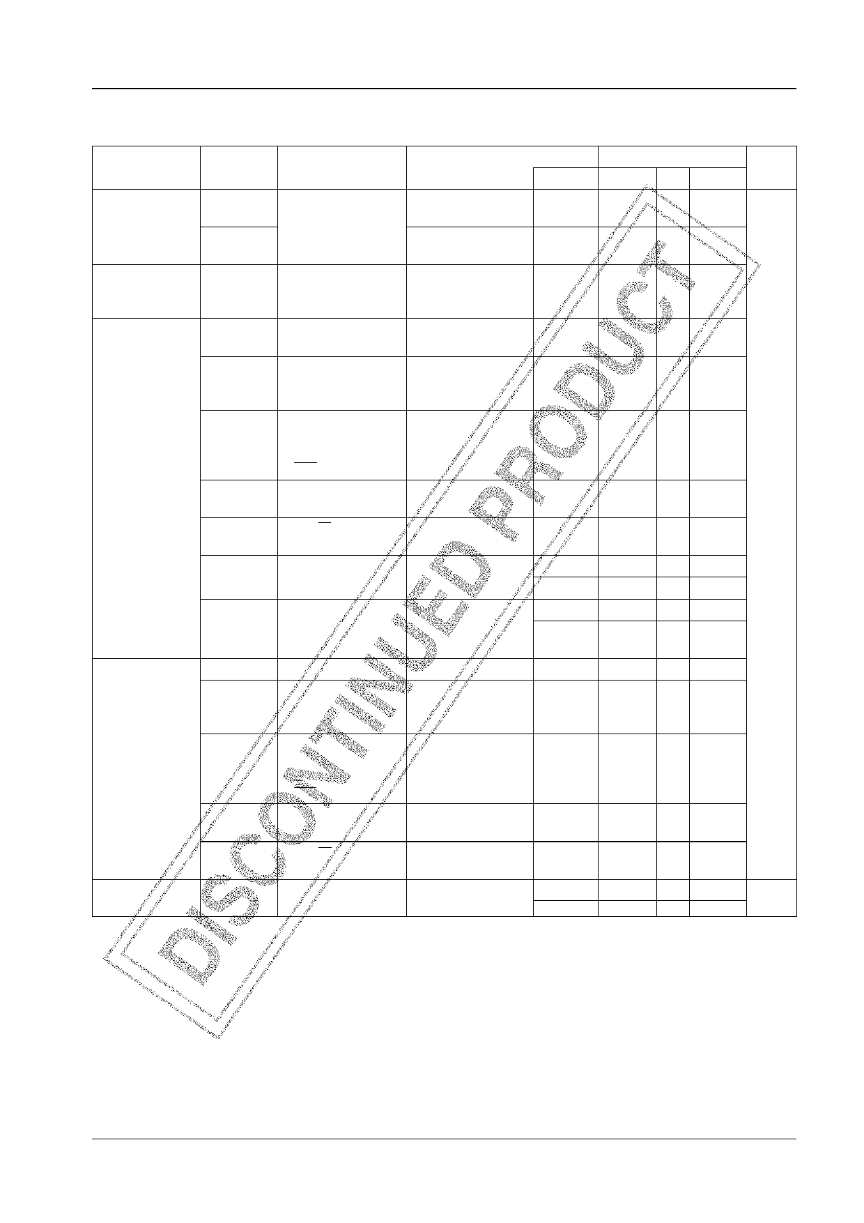
2. Recommended Operating Ranges at Ta = –30°C to +70°C, VSS = 0 V
Parameter
Operating voltage
range
HOLD voltage
Input high voltage
Input low voltage
Operating cycle
time
Symbol
VDD(1)
VDD(2)
VHD
VIH(1)
VIH(2)
VIH(3)
VIH(4)
VIH(5)
VIH(6)
VIH(7)
VIL(1)
VIL(2)
VIL(3)
VIL(4)
VIL(5)
tCYC
Pins
Conditions
Ratings
Unit
VDD[V]
min typ max
VDD
0.98 µs ≤ tCYC
tCYC ≤ 400 µs
4.5
6.0 V
3.9 µs ≤ tCYC
tCYC ≤ 400 µs
2.7
6.0
VDD
RAM and Registers
2.0
6.0
hold voltage at HOLD
mode.
Port 0 (Schmitt)
Output disable
2.7 to 6.0 0.4VDD
VDD
+0.9
• Ports 1, 2
Output disable
2.7 to 6.0 0.75VDD
VDD
• Ports 72, 73
(Schmitt)
• Port 70
Output N-channel
2.7 to 6.0 0.75VDD
VDD
Port input/interrupt transistor OFF
• Port 71
• RES (Schmitt)
Port 70
Output N-channel
2.7 to 6.0 0.9VDD
VDD
Watchdog timer
transistor OFF
• Port 74
• Port 8
Output N-channel
27 to 6.0 0.75VDD
VDD
transistor OFF
Ports 3, 4, 5 of CMOS Output disable
4.0 to 6.0 0.75VDD
VDD
output (Schmitt)
2.7 to 4.0 0.8VDD
VDD
Ports 3, 4, 5 of open-
drain output
(Schmitt)
Output disable
4.0 to 6.0
2.7 to 4.0
0.75VDD
0.8VDD
13.5
13.5
Port 0 (Schmitt)
Output disable
2.7 to 6.0
VSS
• Ports 1, 2, 3, 4, 5
• Ports 72, 73
(Schmitt)
Output disable
2.7 to 6.0
VSS
• Port 70
N-channel transistor 2.7 to 6.0
VSS
Port input/interrupt OFF
• Port 71
• RES (Schmitt)
Port 70
N-channel transistor 2.7 to 6.0
VSS
Watchdog timer
OFF
• Port 74
• Port 8
Output N-channel
2.7 to 6.0
VSS
transistor OFF
4.5 to 6.0
2.7 to 6.0
0.98
3.9
0.2VDD
0.25VDD
0.25VDD
0.8VDD
–1.0
0.25VDD
400 µs
400
No. 5650-11/21
Share Link: 