M62030FP 查看數據表(PDF) - Renesas Electronics
零件编号
产品描述 (功能)
比赛名单
M62030FP Datasheet PDF : 7 Pages
| |||
M62030FP
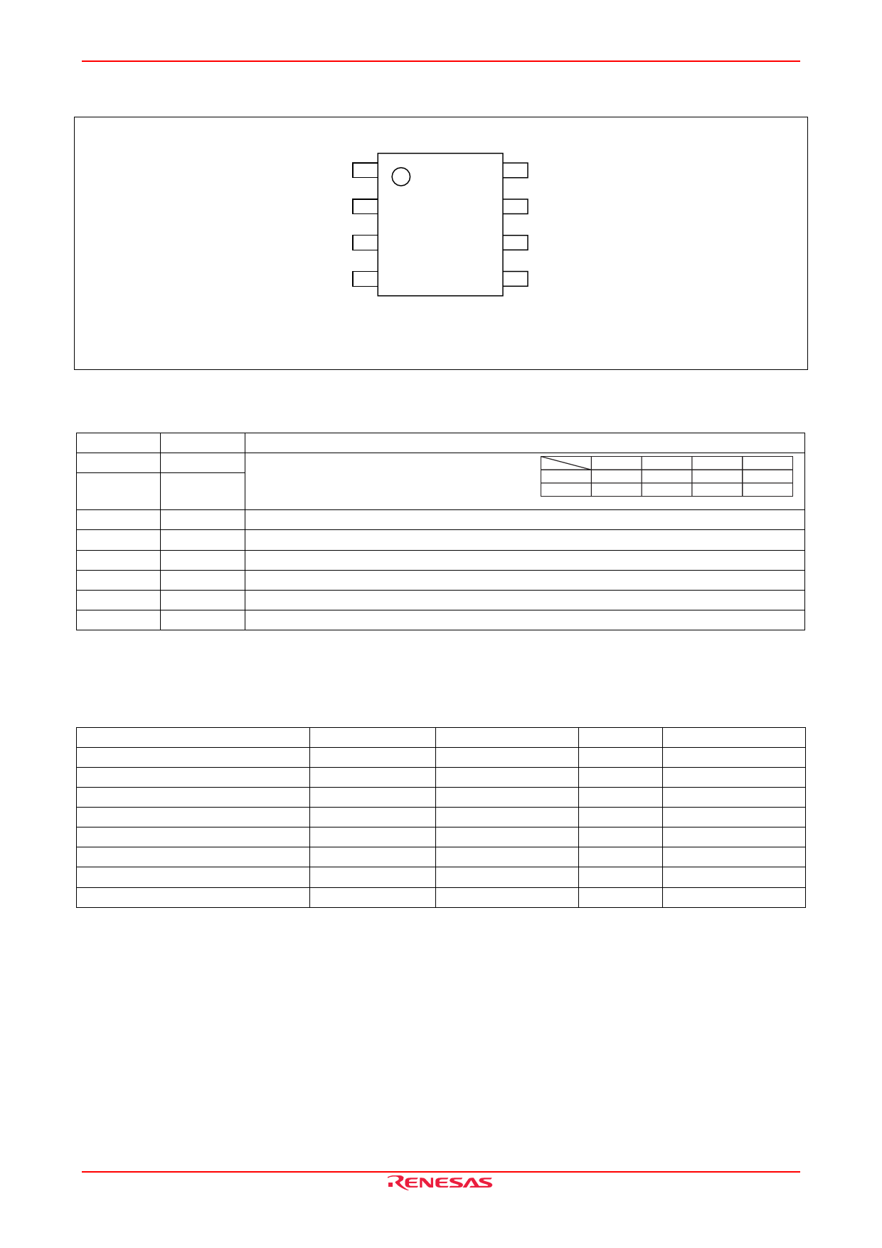
Pin Arrangement
M62030FP
Ct0 1
VIN 2
Ct1 3
8 VRES
7 VCC
6 OUT1
GND 4
5 OUT2
(Top view)
Outline: PRSP0008DE-C (recommend)
PRSP0008DA-A (8P2S-A) (not recommend for new design)
Pin Description
Pin No.
1
3
Symbol
Ct0
Ct1
2
VIN
4
GND
6
OUT1
5
OUT2
7
VCC
8
VRES
Functional Description
Setting delay time.
It is possible to set four kinds of delay times
by inputting “H” or “L” into these two terminal.
25 ms 50 ms 100 ms 200 ms
Ct0
L
H
H
L
Ct1
H
L
H
L
Detecting voltage input
Ground
Output terminal 1 (Delay time 200 µs settlement output)
Output terminal 2 (Delay time variable type output)
Supply voltage
It outputs “L” and “H” to OUT2 terminal when the VRES input is “H” and “L”, respectively.
Absolute Maximum Ratings
Item
Supply voltage
Output sink current
Output voltage
Self reset input voltage
Power dissipation
Thermal derating
Operating temperature
Storage temperature
Symbol
VCC
Isink1, 2
VO
VRES
Pd
Kθ
Topr
Tstg
Rating
–0.3 to +10
8.0
–0.3 to +10
–0.3 to +10
300
3.0
–20 to +75
–40 to +125
(Ta = 25°C, unless otherwise noted)
Unit
Conditions
V
mA
Output1, 2
V
V
mW
mW/°C Ta ≥ 25°C
°C
°C
REJ03D0785-0200 Rev.2.00 Jun 15, 2007
Page 2 of 6
Share Link: 