MC74HCT04A(2015) 查看數據表(PDF) - ON Semiconductor
零件编号
产品描述 (功能)
比赛名单
MC74HCT04A Datasheet PDF : 5 Pages
| |||
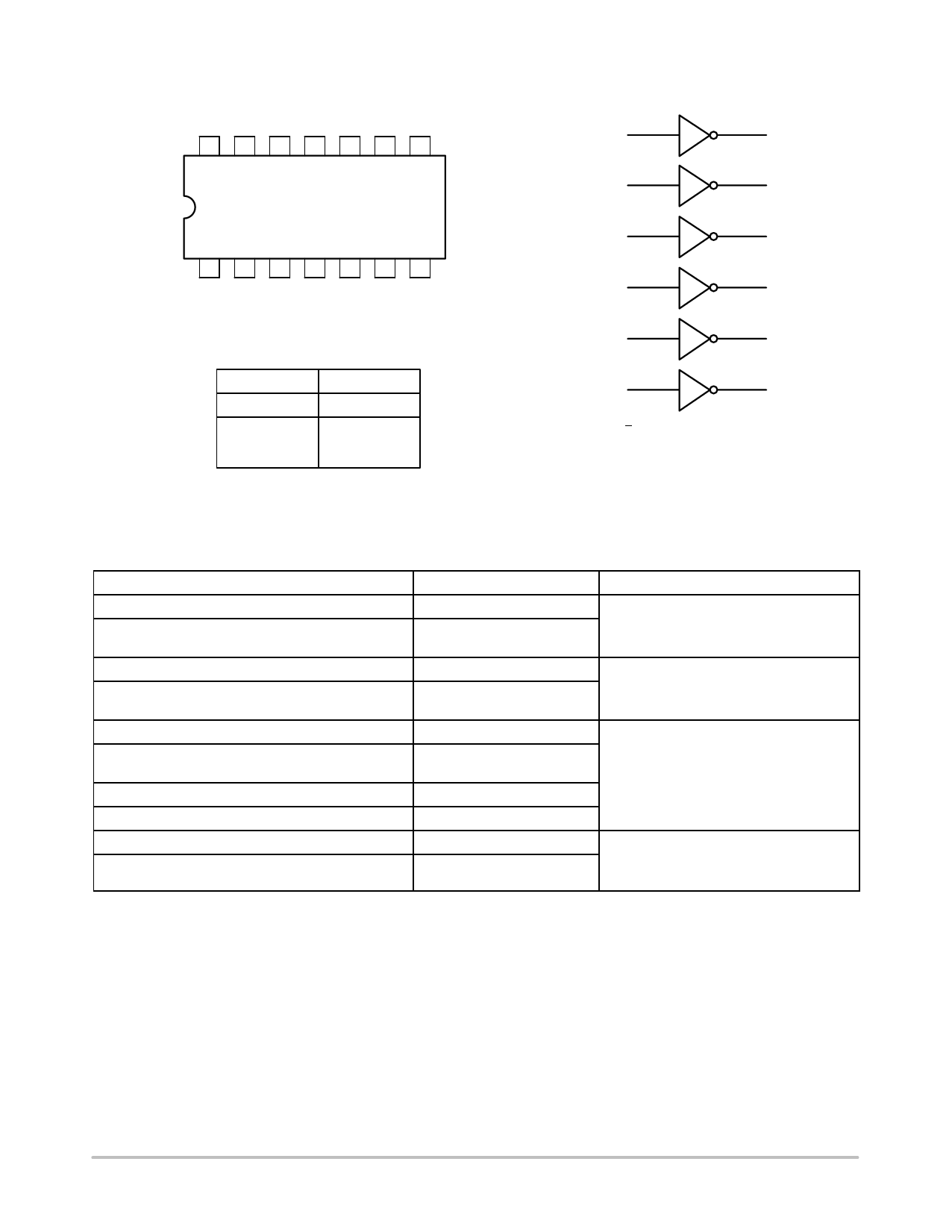
MC74HCT04A
MAXIMUM RATINGS
Symbol
Parameter
Value
Unit
VCC DC Supply Voltage (Referenced to GND)
–0.5 to +7.0
V
Vin DC Input Voltage (Referenced to GND)
–0.5 to VCC + 0.5 V
Vout DC Output Voltage (Referenced to GND)
–0.5 to VCC + 0.5 V
Iin
DC Input Current, per Pin
±20
mA
Iout DC Output Current, per Pin
±25
mA
ICC DC Supply Current, VCC and GND Pins
±50
mA
PD Power Dissipation in Still Air
SOIC Package†
500
mW
TSSOP Package†
450
Tstg Storage Temperature Range
–65 to +150
_C
TL Lead Temperature, 1 mm from Case for 10 Seconds
_C
SOIC or TSSOP Package
260
Stresses exceeding those listed in the Maximum Ratings table may damage the device. If any of
these limits are exceeded, device functionality should not be assumed, damage may occur and
reliability may be affected.
†Derating: SOIC Package: –7 mW/_C from 65_ to 125_C
TSSOP Package: −6.1 mW/_C from 65_ to 125_C
This device contains protection
circuitry to guard against damage
due to high static voltages or electric
fields. However, precautions must
be taken to avoid applications of any
voltage higher than maximum rated
voltages to this high−impedance cir-
cuit. For proper operation, Vin and
Vout should be constrained to the
range GND v (Vin or Vout) v VCC.
Unused inputs must always be
tied to an appropriate logic voltage
level (e.g., either GND or VCC).
Unused outputs must be left open.
RECOMMENDED OPERATING CONDITIONS
Symbol
Parameter
Min
Max
Unit
VCC DC Supply Voltage (Referenced to GND)
4.5
5.5
V
Vin, Vout DC Input Voltage, Output Voltage (Referenced to GND)
0
VCC
V
TA Operating Temperature Range, All Package Types
–55
+125
_C
tr, tf Input Rise/Fall Time (Figure 1)
0
500
ns
Functional operation above the stresses listed in the Recommended Operating Ranges is not implied. Extended exposure to stresses beyond
the Recommended Operating Ranges limits may affect device reliability.
DC CHARACTERISTICS (Voltages Referenced to GND)
Symbol
Parameter
Condition
VCC
Guaranteed Limit
V −55 to 25°C ≤85°C ≤125°C Unit
VIH
Minimum High−Level Input Voltage Vout = 0.1V
4.5
|Iout| ≤ 20mA
5.5
VIL
Maximum Low−Level Input Voltage Vout = VCC − 0.1V
4.5
|Iout| ≤ 20mA
5.5
VOH
Minimum High−Level Output
Vin = VIL
4.5
Voltage
|Iout| ≤ 20mA
5.5
Vin = VIL
|Iout| ≤ 4.0mA 4.5
VOL
Maximum Low−Level Output
Vin = VIH
4.5
Voltage
|Iout| ≤ 20mA
5.5
Vin = VIH
|Iout| ≤ 4.0mA 4.5
Iin
Maximum Input Leakage Current
Vin = VCC or GND
5.5
ICC
Maximum Quiescent Supply
Vin = VCC or GND
5.5
Current (per Package)
Iout = 0mA
2.0
2.0
0.8
0.8
4.4
5.4
3.98
0.1
0.1
0.26
±0.1
1
2.0
2.0
V
2.0
2.0
0.8
0.8
V
0.8
0.8
4.4
4.4
V
5.4
5.4
3.84 3.70
0.1
0.1
V
0.1
0.1
0.33 0.40
±1.0
±1.0
mA
10
40
mA
DICC
Additional Quiescent Supply
Current
Vin = 2.4V, Any One Input
≥ −55°C
Vin = VCC or GND, Other Inputs
Iout = 0mA
5.5
2.9
25 to 125°C
2.4
mA
Product parametric performance is indicated in the Electrical Characteristics for the listed test conditions, unless otherwise noted. Product
performance may not be indicated by the Electrical Characteristics if operated under different conditions.
1. Total Supply Current = ICC + ΣDICC.
www.onsemi.com
2
Share Link: 