MC74HCT240 查看數據表(PDF) - Motorola => Freescale
零件编号
产品描述 (功能)
比赛名单
MC74HCT240
Motorola => Freescale

MC74HCT240 Datasheet PDF : 7 Pages
| |||
MC74HCT240A
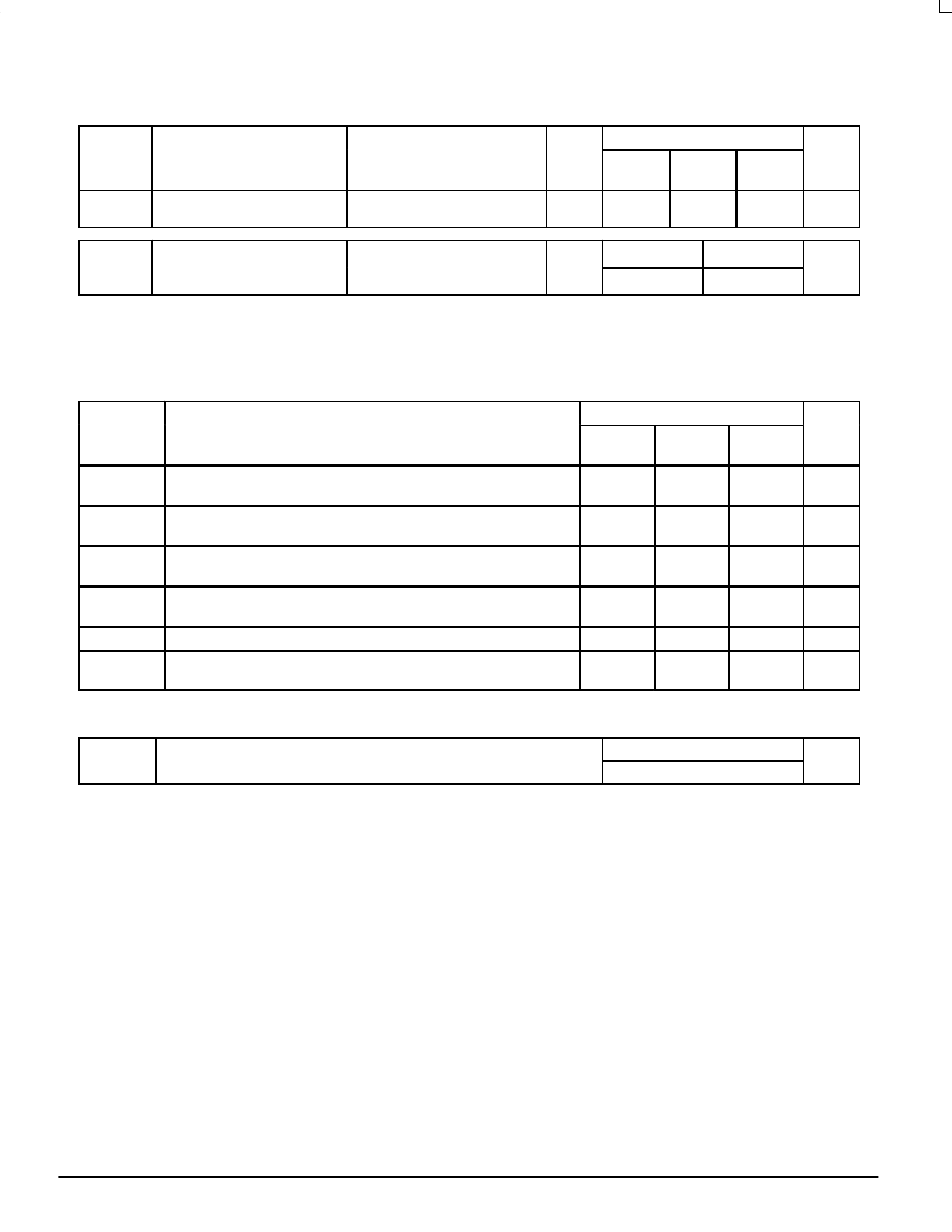
DC ELECTRICAL CHARACTERISTICS (Voltages Referenced to GND)
ÎÎÎÎÎÎÎÎÎÎÎÎÎÎÎÎÎÎÎÎÎÎÎÎÎÎÎÎÎÎÎÎÎÎÎÎÎÎÎÎÎÎÎÎÎÎÎÎÎÎÎÎÎÎÎÎÎÎÎÎÎÎÎÎÎÎÎÎÎÎÎÎÎÎÎÎÎÎÎÎÎÎÎÎÎÎÎÎÎÎÎÎÎÎÎÎÎÎÎ Symbol
ÎÎÎÎÎÎÎÎÎÎÎÎÎÎÎÎÎÎÎÎÎÎÎÎÎÎÎÎÎÎÎÎÎ ICC
Parameter
Maximum Quiescent Supply
Current (per Package)
ÎÎÎÎÎÎÎÎÎÎÎÎÎÎÎÎÎÎÎÎÎÎÎÎÎÎÎÎÎÎÎÎÎÎÎÎÎÎÎÎÎÎÎÎÎÎÎÎÎÎÎÎÎÎÎÎÎÎÎÎÎÎÎÎÎÎÎÎÎÎÎÎÎÎÎÎÎÎÎÎÎÎÎÎÎÎÎÎÎÎÎÎÎÎÎÎÎÎÎÎÎÎÎÎÎÎÎÎÎÎÎÎÎÎÎÎÎÎÎÎÎÎÎÎÎÎÎÎÎÎÎÎ ∆ICC
Additional Quiescent Supply
Current
Test Conditions
Vin = VCC or GND
Iout = 0 µA
Vin = 2.4 V, Any One Input
Vin = VCC or GND, Other Inputs
lout = 0 µA
VCC
V
5.5
5.5
Guaranteed Limit
v v – 55 to
25_C
85_C
125_C Unit
4
40
160
µA
≥ –55_C
2.9
25_C to 125_C
2.4
mA
NOTES:
1. Information on typical parametric values along with frequency or heavy load considerations can be found in Chapter 2 of the Motorola High–
Speed CMOS Data Book (DL129/D).
2. Total Supply Current = ICC + Σ∆ICC.
AC ELECTRICAL CHARACTERISTICS (VCC = 5.0 V ± 10%, CL = 50 pF, Input tr = tf = 6 ns)
Guaranteed Limit
ÎÎÎÎÎÎÎÎÎÎÎÎÎÎÎÎÎÎÎÎÎÎÎÎÎÎÎÎÎÎÎÎÎÎÎÎÎÎÎÎÎÎÎÎÎÎÎÎÎÎÎÎÎÎÎÎÎÎÎÎÎÎÎÎÎÎ Symbol
Parameter
– 55 to
25_C
v v 85_C
125_C Unit
ÎÎÎÎÎÎÎÎÎÎÎÎÎÎÎÎÎÎÎÎÎÎÎÎÎÎÎÎÎÎÎÎÎ tPLH,
ÎÎÎÎÎÎÎÎÎÎÎÎÎÎÎÎÎÎÎÎÎÎÎÎÎÎÎÎÎÎÎÎÎ tPHL
Maximum Propagation Delay, A to YA or B to YB
(Figures 1 and 3)
20
25
30
ns
ÎÎÎÎÎÎÎÎÎÎÎÎÎÎÎÎÎÎÎÎÎÎÎÎÎÎÎÎÎÎÎÎÎ tPLZ,
ÎÎÎÎÎÎÎÎÎÎÎÎÎÎÎÎÎÎÎÎÎÎÎÎÎÎÎÎÎÎÎÎÎ tPHZ
Maximum Propagation Delay, Output Enable to YA or YB
(Figures 2 and 4)
28
35
42
ns
ÎÎÎÎÎÎÎÎÎÎÎÎÎÎÎÎÎÎÎÎÎÎÎÎÎÎÎÎÎÎÎÎÎ tPZL,
tPZH
Maximum Propagation Delay, Output Enable to YA or YB
(Figures 2 and 4)
25
31
38
ns
ÎÎÎÎÎÎÎÎÎÎÎÎÎÎÎÎÎÎÎÎÎÎÎÎÎÎÎÎÎÎÎÎÎ tTLH,
ÎÎÎÎÎÎÎÎÎÎÎÎÎÎÎÎÎÎÎÎÎÎÎÎÎÎÎÎÎÎÎÎÎ tTHL
Maximum Output Transition Time, Any Output
(Figures 1 and 3)
12
15
18
ns
ÎÎÎÎÎÎÎÎÎÎÎÎÎÎÎÎÎÎÎÎÎÎÎÎÎÎÎÎÎÎÎÎÎ Cin
Maximum Input Capacitance
10
10
10
pF
ÎÎÎÎÎÎÎÎÎÎÎÎÎÎÎÎÎÎÎÎÎÎÎÎÎÎÎÎÎÎÎÎÎ Cout
Maximum Three–State Output Capacitance (Output in High–Impedance
15
15
15
pF
ÎÎÎÎÎÎÎÎÎÎÎÎÎÎÎÎÎÎÎÎÎÎÎÎÎÎÎÎÎÎÎÎÎ State)
ÎÎÎÎÎÎÎÎÎÎÎÎÎÎÎÎÎÎÎÎÎÎÎÎÎÎÎÎÎÎÎÎÎ NOTE: For propagation delays with loads other than 50 pF, and information on typical parametric values, see Chapter 2 of the Motorola High–
Speed CMOS Data Book (DL129/D).
Typical @ 25°C, VCC = 5.0 V
CPD
Power Dissipation Capacitance (Per Enabled Output)*
55
pF
* Used to determine the no–load dynamic power consumption: PD = CPD VCC2f + ICC VCC. For load considerations, see Chapter 2 of the
Motorola High–Speed CMOS Data Book (DL129/D).
High–Speed CMOS Logic Data
3
DL129 — Rev 6
MOTOROLA
Share Link: