MX10E8050IA 查看數據表(PDF) - Macronix International
零件编号
产品描述 (功能)
比赛名单
MX10E8050IA Datasheet PDF : 88 Pages
| |||
PRELIMINARY
MX10E8050I /
MX10E8050IA
FEATURES
- 80C51 CPU core
- 3.0 ~ 3.6V voltage range
- On-chip Flash program memory with in-system
programming ( ISP )
- Operating frequency up to 40MHz (12x), 20MHz(6x)
- 64K bytes Flash memory for code memory
- 1280 bytes internal data RAM
- Low power consumption
- Code and data memory expandable to 64K Bytes
- Four 8 bit and one 4 bit general purpose I/O ports
- Three standard 16-bit Timers
- In - Application Programming( IAP ) capability
- On-chip Watch Dog Timer
- Four channel PWM outputs/4bit general purpose I/O
ports ( PLCC & LQFP only )
- UART
- 7 interrupt sources with four priority level
- 5 volt tolerant input
- 400kb/s I2C
- 6x / 12x clock mode
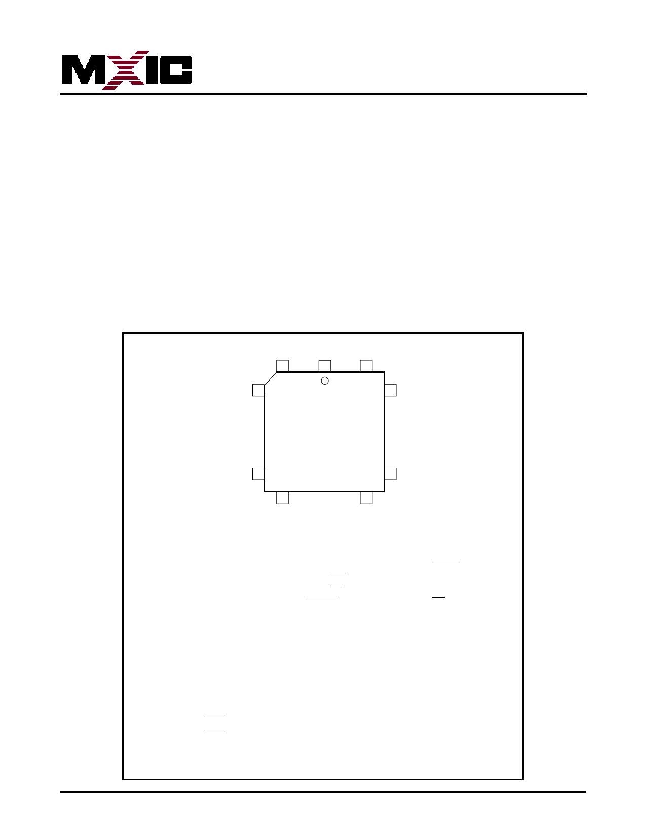
PIN Configurations
6
1
40
7
39
PLCC44
17
29
Pin Function
1 P4.2/PWM2
2 P1.0/T2
3 P1.1/T2EX
4 P1.2
5 P1.3
6 P1.4
7 P1.5
8 P1.6/SCL
9 P1.7/SDA
10 RST
11 P3.0/RxD
12 P4.3/PWM3
13 P3.1/TxD
14 P3.2/INT0
15 P3.3/INT1
18
28
Pin Function
16 P3.4/T0
17 P3.5/T1
18 P3.6/WR
19 P3.7/RD
20 XTAL2
21 XTAL1
22 VSS
23 P4.0/PWM0
24 P2.0/A8
25 P2.1/A9
26 P2.2/A10
27 P2.3/A11
28 P2.4/A12
29 P2.5/A13
30 P2.6/A14
Pin Function
31 P2.7/A15
32 PSEN
33 ALE
34 P4.1/PWM1
35 EA
36 P0.7/AD7
37 P0.6/AD6
38 P0.5/AD5
39 P0.4/AD4
40 P0.3/AD3
41 P0.2/AD2
42 P0.1/AD1
43 P0.0/AD0
44 VCC
P/N:PM0887 Specifications subject to change without notice, contact your sales representatives for the most update information. REV. 1.6, MAR. 28, 2005
2
Share Link: 