PI74FCT163244 查看數據表(PDF) - Pericom Semiconductor
零件编号
产品描述 (功能)
比赛名单
PI74FCT163244 Datasheet PDF : 5 Pages
| |||
PI74FCT163244
1122334455667788990011223344556677889900112233445566778899001122112233445566778899001122334455667788990011223344556677889900112211223344556677889900112233445566778899001122334435566.77388V99001112211622-33B445566I77T889900B1122U3344F5566F7788E9900R1122/33L4455I66N778899E0011D221122R3344I55V6677E8899R001122
Maximum Ratings
(Above which the useful life may be impaired. For user guidelines, not tested.)
Storage Temperature .......................................................... 65°C to +150°C
Ambient Temperature with Power Applied ......................... 40°C to +85°C
Supply Voltage to Ground Potential (Inputs & Vcc Only) ... 0.5V to +7.0V
Supply Voltage to Ground Potential (Outputs & D/O Only) 0.5V to +7.0V
DC Input Voltage .................................................................. 0.5V to +7.0V
DC Output Current ............................................................................ 120 mA
Power Dissipation .................................................................................. 1.0W
Note:
Stresses greater than those listed under MAXIMUM
RATINGS may cause permanent damage to the de-
vice. This is a stress rating only and functional opera-
tion of the device at these or any other conditions
above those indicated in the operational sections of
this specification is not implied. Exposure to absolute
maximum rating conditions for extended periods may
affect reliability.
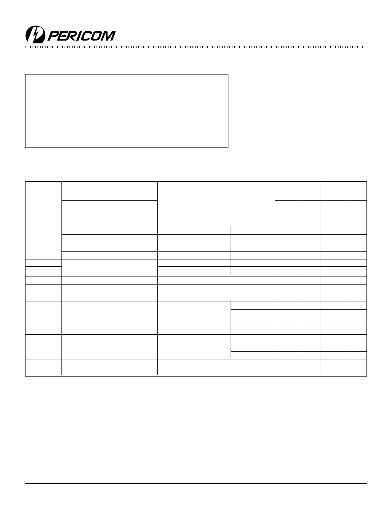
DC Electrical Characteristics (Over the Operating Range, TA = –40°C to +85°C, VCC = 2.7V to 3.6V)
Parameters
Description
Test Conditions(1)
Min. Typ(2) Max. Units
VIH
Input HIGH Voltage (Input pins) Guaranteed Logic HIGH Level
2.2
5.5
V
Input HIGH Voltage (I/O pins)
2.0 Vcc+0.5 V
VIL
Input LOW Voltage
(Input and I/O pins)
Guaranteed Logic LOW Level
0.5 0.8
V
IIH
Input HIGH Current (Input pins) VCC = Max.
VIN = 5.5V
±1 µA
Input HIGH Current (I/O pins) VCC = Max.
VIN = VCC
±1 µA
IIL
Input LOW Current (Input pins) VCC = Max.
VIN = GND
±1 µA
Input LOW Current (I/O pins)
VCC = Max.
VIN = GND
±1 µA
IOZH
High Impedance Output Current VCC = Max.
VOUT = VCC
±1
µA
IOZL
(3-State Output pins)
VCC = Max.
VOUT = GND
±1
µA
VIK
IODH
IODL
Clamp Diode Voltage
Output HIGH Current
Output LOW Current
VCC = Min., IIN = 18 mA
0.7 1.2 V
VCC = 3.3V, VIN = VIH or VIL, VO = 1.5V(3) 36 60 110 mA
VCC = 3.3V, VIN = VIH or VIL, VO = 1.5V(3) 50
90 200 mA
VOH
Output HIGH Voltage
VCC = Min.
IOH = 0.1mA Vcc-0.2
V
VIN = VIH or VIL
VCC = 3.0V,
IOH = 3mA
2.4 3.0
V
IOH = 8mA
2.4(5) 3.0
V
VIN = VIH OR VIL
IOH = 24mA 2.0
V
VOL
Output LOW Voltage
VCC = Min.
IOL = 0.1mA
0.2
V
VIN = VIH or VIL
IOL = 16mA
0.2 0.4
V
IOS
Short Circuit Current(4)
IOL = 24mA
VCC = Max.(3), VOUT = GND
0.3 0.5
V
60 85 240 mA
VH
Input Hysteresis
150 mV
Notes:
1. For Max. or Min. conditions, use appropriate value specified under Electrical Characteristics for the applicable device type.
2. Typical values are at VCC = 3.3V, +25°C ambient and maximum loading.
3. Not more than one output should be shorted at one time. Duration of the test should not exceed one second.
4. This parameter is guaranteed but not tested.
5. VOH = VCC 0.6V at rated current.
3
PS2052B 01/18/99
Share Link: 