SPT7937SIR 查看數據表(PDF) - Unspecified
零件编号
产品描述 (功能)
比赛名单
SPT7937SIR Datasheet PDF : 11 Pages
| |||
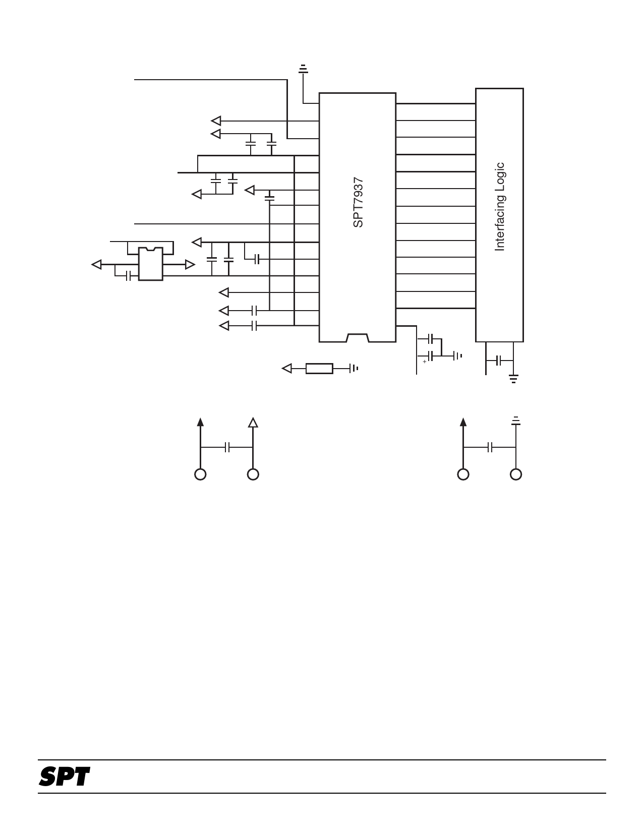
Figure 2 – Typical Interface Circuit
CLK IN
+
+A5
+
AIN
+A5
U1
+
TK11240B
Ext VREF
(+4 V)
OGND
DGND
OTR
D11
Out of Range Bit
MSB
CLK
D10
DVDD
D9
AVDD
D8
DGNUD1
D7
(DUT)
VINR
D6
VIN
D5
RGND
D4
VRHS
D3
VRHF
D2
VRLF
D1
VRLS
D0
LSB
28 DVDD2 OVDD 1
FB
+D3/5V
+D3/5V
+A5
+D3/5
+
10 µF
+
10 µF
+A5 AGND
Notes:
1) Unless otherwise specified, all non-polarized capacitors are 0.01 microfarad
surface-mount chip capacitors. They need to be placed as close to the pin as possible
2) All polarized capacitors are 4.7 to 10 microfarad tantalum surface-mount capacitors
3) FB is a ferrite bead. Place FB as close to the DUT as possible
4) U1 is TOKO regulator TK11240B (4.0 V)
+D3/5
DGND
TYPICAL INTERFACE CIRCUIT
Very few external components are required to achieve the
stated device performance. Figure 2 shows the typical inter-
face requirements when using the SPT7937 in normal
circuit operation. The following sections provide descrip-
tions of the major functions and outline critical performance
criteria to consider for achieving the optimal device
performance.
POWER SUPPLIES AND GROUNDING
SPT suggests that both the digital (DVDD) and the analog
(AVDD) supply voltages on the SPT7937 be derived from a
single analog supply as shown in figure 2. A separate digital
supply should be used for the digital output driver supply
(OVDD) and all interface circuitry. SPT suggests using this
power supply configuration to prevent a possible latch-up
condition on power up. In addition, the power supplies must
be powered up before the analog input is applied.
SPT
6
SPT7937
1/14/00
Share Link: 