V6319LSP3B 查看數據表(PDF) - EM Microelectronic - MARIN SA
零件编号
产品描述 (功能)
比赛名单
V6319LSP3B Datasheet PDF : 6 Pages
| |||
R
Application Information
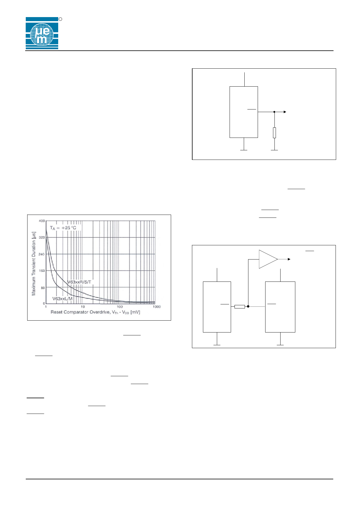
Negative-Going VDD Transients
In addition to issuing a reset to the microprocessor during
power-up, power-down and brownout conditions, the
V6309/V6319 are relatively immune to short duration
negative-doing VDD transients (glitches). Fig. 8 shows
typical transient duration vs. Reset comparator overdrive,
for which the V6309/V6319 do not generate a reset pulse.
The graph was generated using a negative-going pulse
applied to VDD, starting 0.5V above the actual reset
threshold and ending below it by the magnitude indicated
(reset comparator overdrive). The graph indicates the
maximum pulse width a negative-going VDD transient can
have without causing a reset pulse. As the magnitude of
the transient increases (goes farther below the reset
threshold), the maximum allowable pulse width decreases.
Typically, for the V6309L and V6319M, a VDD transient that
goes 100V below the reset threshold and lasts 20µs or less
will not cause a reset pulse. A 0.1µF bypass capacitor
mounted as close as possible to the VDD pin provides
additional transient immunity.
Max. Transient Duration without causing a Reset Pulse
versus Reset Comparator Overdrive
Fig .9
Ensuring a Valid Reset Output down to VDD = 0V
When VDD falls below 1V, the V6309 RESET output no
longer sinks current, it becomes an open circuit.
Therefore, high-impedance CMOS logic inputs connected
to RESET can drift to undetermined voltages. This
presents no problem in most applications, since most µP
and other circuitry is inoperative with VDD below 1V.
However, in applications where RESET must be valid
down to 0V, adding a pull-down resistor to RESET causes
any stray leakage currents to flow to ground, holding
RESET low (Fig. 10). R1's value is not critical; 100 kΩ is
large enough not to load RESET and small enough to pull
RESET to ground. A 100 kΩ pull-up resistor to VDD is also
recommended for the V6319, if RESET is required to
remain valid for VDD < 1V.
V6309
V6319
RESET Valid for VDD = Ground Circuit
VDD
RES
V6309
VSS
100 kΩ
Fig. 10
Interfacing to µPs with Bidirectional Reset Pins
Microprocessors with bidirectional reset pins (such as the
Motorola 68HC11 series) can connect to the V6309 reset
output. If, for example, the V6309 RESET output is
asserted high and the µP wants to pull it low, indeterminate
logic levels may result. To correct this, connect a 4.7 kΩ
resistor between the V6309 RESET and the µP reset I/O
(Fig. 11). Buffer the V6309 RESET output to other system
components.
Interfacing to µPs with Bidirectional Reset I/O
Buffer
Buffer RES to
other system
components
VDD
VDD
RES
V6309
VSS
44..77kkΩO
RES
µP
VSS
Fig. 11
Benefits of Highly Accurate Reset Threshold
Most µP supervisor ICs have reset threshold voltages
between 5% and 10% below the value of nominal supply
voltages. This ensures a reset will not occur within 5% of
the nominal supply, but will occur when the supply is 10%
below nominal. When using ICs rated at only the nominal
supply ±5%, this leaves a zone of uncertainty where the
supply is between 5% and 10% low, and where the reset
may or may not be asserted.
The V6209/T and V6319/T use highly accurate circuitry to
ensure that reset is asserted close to the 5% limit, and long
before the supply has declined to 10% below nominal.
Copyright © 2006, EM Microelectronic-Marin SA
4
03/06 – rev.G
www.emmicroelectronic.com
Share Link: 