W83L177R 查看數據表(PDF) - Winbond
零件编号
产品描述 (功能)
比赛名单
W83L177R Datasheet PDF : 9 Pages
| |||
W83L177R
7.0 SPECIFICATIONS
PRELIMINARY
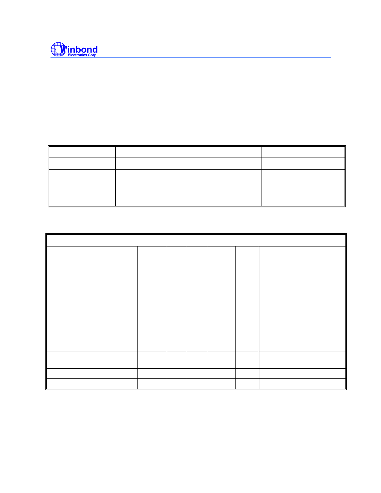
7.1 ABSOLUTE MAXIMUM RATINGS
Stresses greater than those listed in this table may cause permanent damage to the device.
Precautions should be taken to avoid application of any voltage higher than the maximum rated
voltages to this circuit. Maximum conditions for extended periods may affect reliability. Unused
inputs must always be tied to an appropriate logic voltage level (Ground or Vdd).
Symbol
Vdd , VIN
TSTG
TB
TA
Parameter
Voltage on any pin with respect to GND
Storage Temperature
Ambient Temperature
Operating Temperature
Rating
- 0.5 V to + 7.0 V
- 65°C to + 150°C
- 55°C to + 125°C
0°C to + 70°C
7.2 AC CHARACTERISTICS
Vdd = 3.3V ± 5 % , TA = 0°C to +70°C, Test load = 30 pF
Parameter
Symbo Min Typ Max
l
Input frequency
fIN
0
150
Output Rise Time
tR
1.5
4.0
Output Fall Time
tF
1.5
4.0
Output Skew, Rising Edges
tSR
250
Output Skew, Falling Edges
tSF
250
Output Enable Time
tEN
1.0
8.0
Output Disable Time
tDIS
1.0
8.0
Rising Edge Propagation tPR
1.0
Delay
<4.0
Falling Edge Propagation tPF
1.0
Delay
<4.0
Duty Cycle
tD
45
55
AC Output Impedance
ZO
15
Units
Test Conditions
MHz
V/ns
V/ns
ps
ps
ns
ns
ns
Measured from 0.4V to 2.4V
Measured from 0.4V to 2.4V
ns
% Measure at 1.5V
Ω
Publication Release Date: Mar. 1999
-6-
Revision 0.10
Share Link: 