HD74CDCV857A 查看數據表(PDF) - Renesas Electronics
零件编号
产品描述 (功能)
比赛名单
HD74CDCV857A Datasheet PDF : 13 Pages
| |||
HD74CDCV857A
Recommended Operating Conditions
Item
Symbol Min
Typ
Max
Unit Conditions Notes
Output supply voltage
Supply voltage
DC input signal voltage
High level input voltage
Low level input voltage
VDDQ
AVCC
VIN
VIHG
VILG
2.3
VDDQ–0.12
–0.3
1.7
2.5
VDDQ
—
—
–0.3
—
2.7
V
2.7
V
VDDQ+0.3 V All pins
1
VDDQ+0.3 V PWRDWN
input pin
0.7
V PWRDWN
input pin
Input differential voltage VID
0.36
—
VDDQ+0.6 V
3
Output differential voltage VOD
0.70
—
VDDQ+0.6 V
Input differential-pair
VIX
VDDQ/2 –0.2 —
VDDQ/2 +0.2 V
2, 3
cross voltage
Output differential-pair
VOX
VDDQ/2 –0.15 —
VDDQ/2 +0.15 V
2, 3
cross voltage
Output current
IOH
—
—
–12
mA
IOL
—
—
12
mA
Input clock slew rate
tSL(I)
1
—
4
V/ns 20% – 80% 3
Operating temperature
Ta
0
—
70
°C
3
Notes:
Inputs pins must be prevent from floating.
Feedback inputs (FBIN, FBIN) may float when the device is in low power mode.
1. DC input signal voltage specifies the allowable dc execution of differential input.
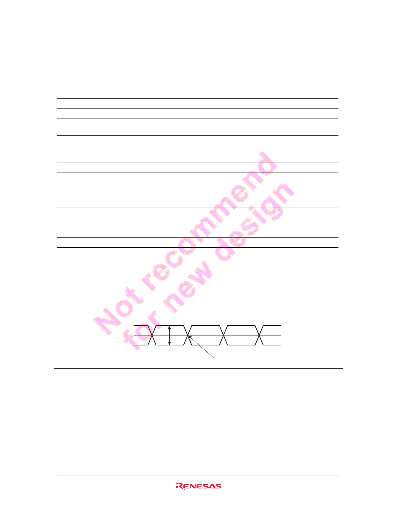
2. Differential cross point voltage is expected to track variations of VDDQ and is the voltage at which
the differential signals must be crossing. (See figure1)
3. Guaranteed by design, not 100% tested in production.
CLK
VID
CLK
Crossing point
Figure 1 Differential input levels
Rev.3.00, Oct.09.2003, page 6 of 12
Share Link: 