AD815A 查看數據表(PDF) - Analog Devices
零件编号
产品描述 (功能)
比赛名单
AD815A Datasheet PDF : 15 Pages
| |||
AD815
SIDE A
SIDE B
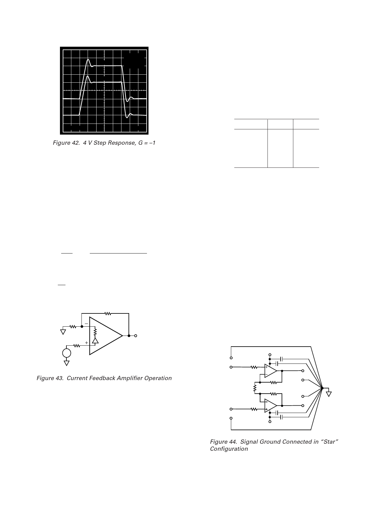
G = –1
RF = 562⍀
RL = 100⍀
Choice of Feedback and Gain Resistors
The fine scale gain flatness will, to some extent, vary with
feedback resistance. It therefore is recommended that once
optimum resistor values have been determined, 1% tolerance
values should be used if it is desired to maintain flatness over
a wide range of production lots. Table I shows optimum values
for several useful configurations. These should be used as
starting point in any application.
1V
20ns
Figure 42. 4 V Step Response, G = –1
THEORY OF OPERATION
The AD815 is a dual current feedback amplifier with high
(500 mA) output current capability. Being a current feedback
amplifier, the AD815’s open-loop behavior is expressed
as transimpedance, ∆VO/∆I–IN, or TZ. The open-loop
transimpedance behaves just as the open-loop voltage gain
of a voltage feedback amplifier, that is, it has a large dc value
and decreases at roughly 6 dB/octave in frequency.
Since RIN is proportional to 1/gM, the equivalent voltage gain is
just TZ × gM, where the gM in question is the transconductance
of the input stage. Using this amplifier as a follower with gain,
Figure 43, basic analysis yields the following result:
( ) VO = G ×
TZ S
( ) VIN
T Z S + G × RIN + RF
where:
G = 1 + RF
RG
RIN = 1/gM ≈ 25 Ω
RF
RG
RIN
RN
VOUT
VIN
Table I. Resistor Values
RF (⍀) RG (⍀)
G = +1 562
ϱ
–1 499
499
+2 499
499
+5 499
125
+10 1 k
110
PRINTED CIRCUIT BOARD LAYOUT
CONSIDERATIONS
As to be expected for a wideband amplifier, PC board parasitics
can affect the overall closed-loop performance. Of concern are
stray capacitances at the output and the inverting input nodes. If
a ground plane is to be used on the same side of the board as
the signal traces, a space (5 mm min) should be left around the
signal lines to minimize coupling.
POWER SUPPLY BYPASSING
Adequate power supply bypassing can be critical when optimizing
the performance of a high frequency circuit. Inductance in the
power supply leads can form resonant circuits that produce
peaking in the amplifier’s response. In addition, if large current
transients must be delivered to the load, then bypass capacitors
(typically greater than 1 µF) will be required to provide the best
settling time and lowest distortion. A parallel combination of
10.0 µF and 0.1 µF is recommended. Under some low frequency
applications, a bypass capacitance of greater than 10 µF may be
necessary. Due to the large load currents delivered by the
AD815, special consideration must be given to careful bypassing.
The ground returns on both supply bypass capacitors as well as
signal common must be “star” connected as shown in Figure 44.
+VS
+IN
Figure 43. Current Feedback Amplifier Operation
Recognizing that G × RIN << RF for low gains, it can be seen to
the first order that bandwidth for this amplifier is independent
of gain (G).
Considering that additional poles contribute excess phase at
high frequencies, there is a minimum feedback resistance below
which peaking or oscillation may result. This fact is used to
determine the optimum feedback resistance, RF. In practice
parasitic capacitance at the inverting input terminal will also add
phase in the feedback loop, so picking an optimum value for RF
can be difficult.
Achieving and maintaining gain flatness of better than 0.1 dB at
frequencies above 10 MHz requires careful consideration of
several issues.
RF
RG
(OPTIONAL)
RF
–IN
–VS
+OUT
–OUT
Figure 44. Signal Ground Connected in “Star”
Configuration
–10–
REV. D
Share Link: 