GS88237BB-250V 查看數據表(PDF) - Giga Semiconductor
零件编号
产品描述 (功能)
比赛名单
GS88237BB-250V Datasheet PDF : 28 Pages
| |||
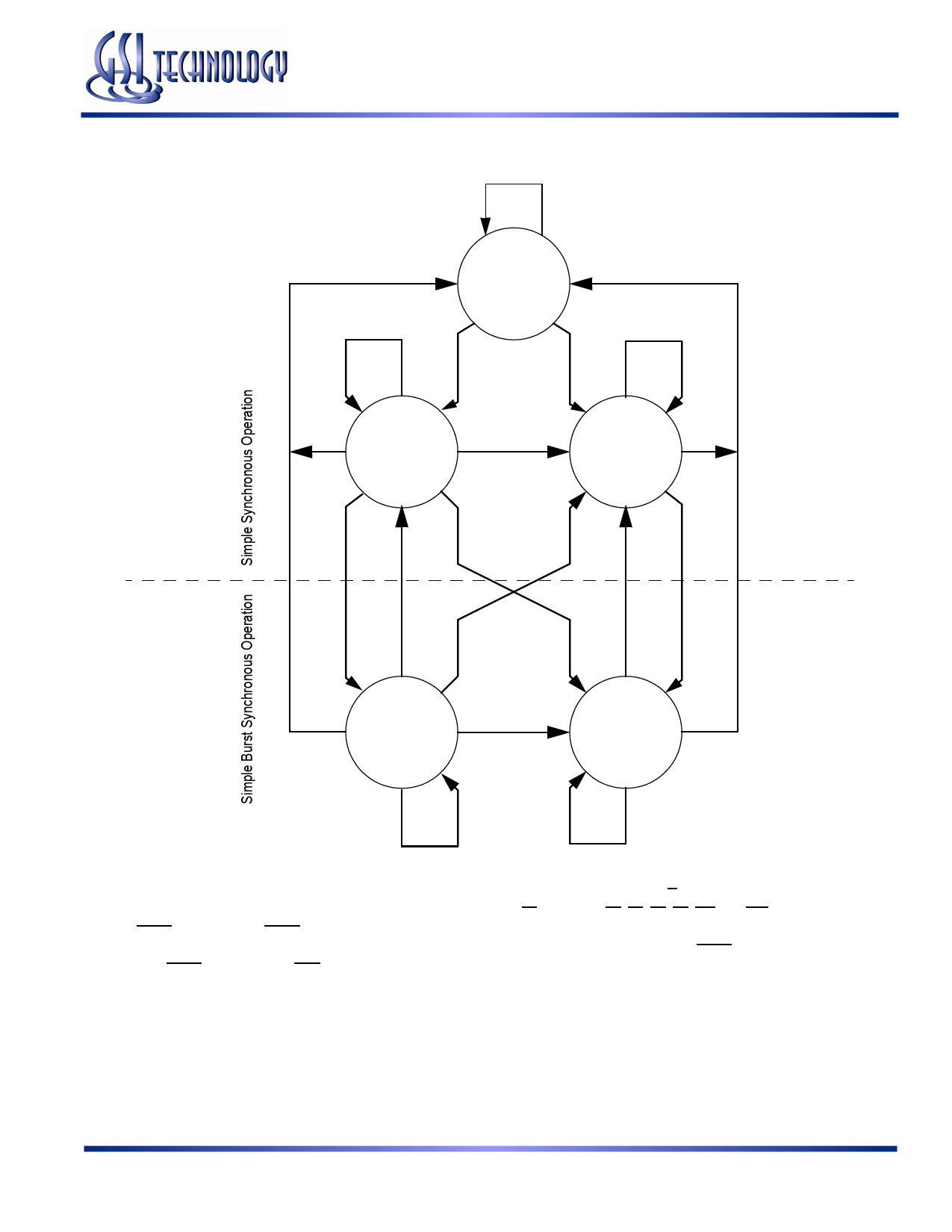
Simplified State Diagram
GS88237BB/D-xxxV
X
Deselect
W
R
W
R
X
First Write R
CW
CR
First Read
X
CR
W
R
X Burst Write
CR
CW
R
Burst Read
X
CR
Notes:
1. The diagram shows only supported (tested) synchronous state transitions. The diagram presumes G is tied low.
2. The upper portion of the diagram assumes active use of only the Enable (E1) and Write (BA, BB, BC, BD, BW, and GW) control inputs, and
that ADSP is tied high and ADSC is tied low.
3. The upper and lower portions of the diagram together assume active use of only the Enable, Write, and ADSC control inputs and
assumes ADSP is tied high and ADV is tied low.
Rev: 1.04 6/2006
9/28
Specifications cited are subject to change without notice. For latest documentation see http://www.gsitechnology.com.
© 2003, GSI Technology
Share Link: 