GS880Z18BGT-150V 查看數據表(PDF) - Giga Semiconductor
零件编号
产品描述 (功能)
比赛名单
GS880Z18BGT-150V Datasheet PDF : 24 Pages
| |||
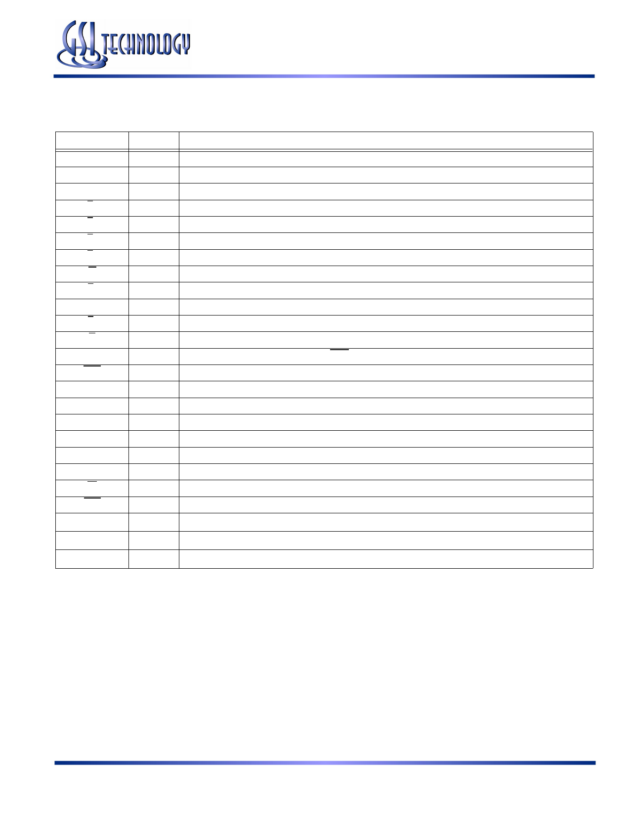
100-Pin TQFP Pin Descriptions
Symbol
A0, A1
A
CK
BA
BB
BC
BD
W
E1
E2
E3
G
ADV
CKE
NC
DQA
DQB
DQ
DQD
ZZ
FT
LBO
VDD
VSS
VDDQ
Type
In
In
In
In
In
In
In
In
In
In
In
In
In
In
—
I/O
I/O
I/O
I/O
In
In
In
In
In
In
GS880Z18/32/36BT-xxxV
Description
Burst Address Inputs; Preload the burst counter
Address Inputs
Clock Input Signal
Byte Write signal for data inputs DQA1–DQA9; active low
Byte Write signal for data inputs DQB1–DQB9; active low
Byte Write signal for data inputs DQC1–DQC9; active low
Byte Write signal for data inputs DQD1–DQD9; active low
Write Enable; active low
Chip Enable; active low
Chip Enable; Active High. For self decoded depth expansion
Chip Enable; Active Low. For self decoded depth expansion
Output Enable; active low
Advance/Load; Burst address counter control pin
Clock Input Buffer Enable; active low
No Connect
Byte A Data Input and Output pins
Byte B Data Input and Output pins
Byte C Data Input and Output pins
Byte D Data Input and Output pins
Power down control; active high
Pipeline/Flow Through Mode Control; active low
Linear Burst Order; active low
Core power supply
Ground
Output driver power supply
Rev: 1.03 6/2006
5/24
Specifications cited are subject to change without notice. For latest documentation see http://www.gsitechnology.com.
© 2001, GSI Technology
Share Link: 