P4C116 查看數據表(PDF) - Semiconductor Corporation
零件编号
产品描述 (功能)
比赛名单
P4C116 Datasheet PDF : 14 Pages
| |||
P4C116/P4C116L
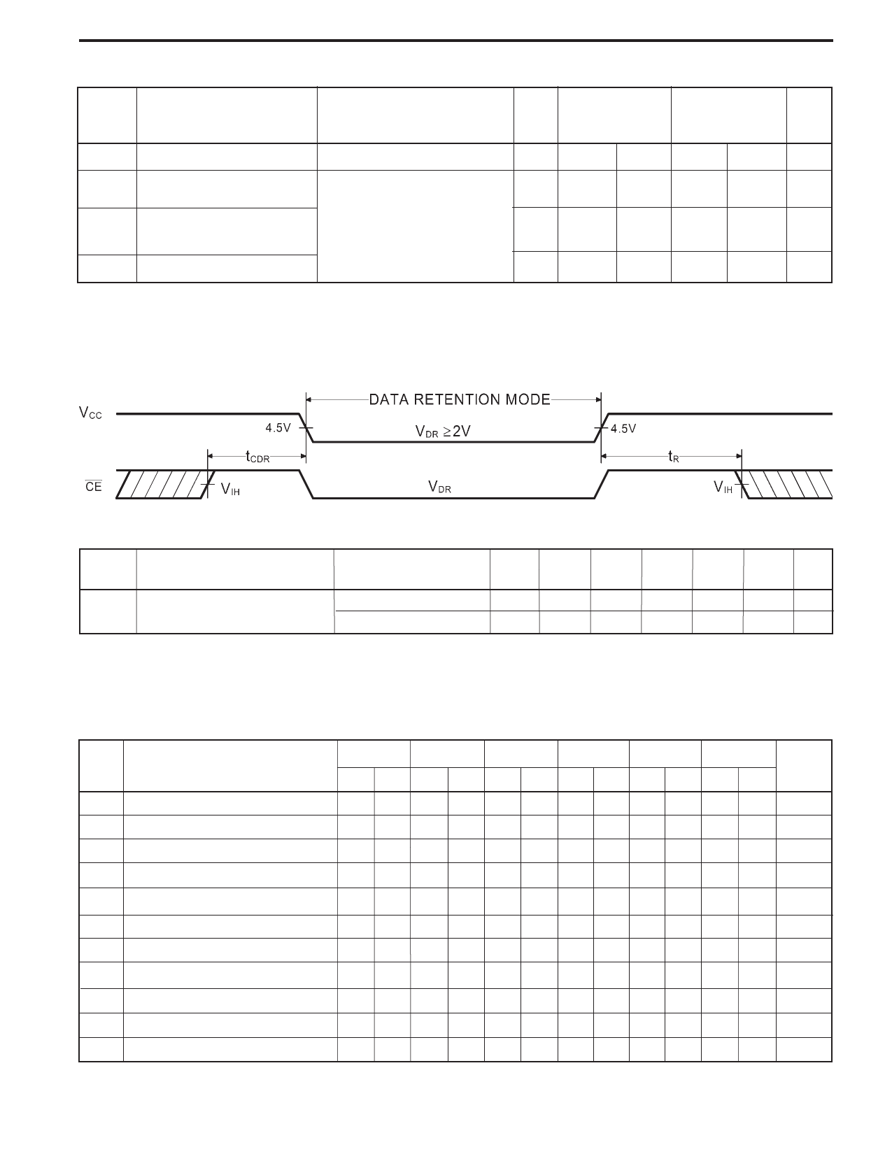
DATA RETENTION CHARACTERISTICS (P4C116L Military Temperature Only)
Symbol
Parameter
VDR
VCC for Data Retention
Test Conditons
Typ.*
Max
Min
VCC =
VCC =
2.0V 3.0V 2.0V 3.0V
2.0
ICCDR Data Retention Current
tCDR
Chip Deselect to
Data Retention Time
tR†
Operation Recovery Time
*TA = +25°C
§tRC = Read Cycle Time
† This parameter is guaranteed but not tested.
CE ≥ VCC –0.2V,
VIN ≥ VCC –0.2V
or VIN ≤ 0.2V
10
0
tRC§
15 600 900
Unit
V
µA
ns
ns
DATA RETENTION WAVEFORM
POWER DISSIPATION CHARACTERISTICS VS. SPEED
Symbol
Parameter
ICC Dynamic Operating Current*
Temperature
Range
Commercial
Military
–10 –12 –15 –20 –25 –35 Unit
180 170 160 155 150 140 mA
N/A N/A 170 160 155 150 mA
*VCC = 5.5V. Tested with outputs open. f = Max. Switching inputs are 0V and 3V. CE = VIL, OE = VIH.
AC ELECTRICAL CHARACTERISTICS—READ CYCLE
(VCC = 5V ± 10%, All Temperature Ranges)(2)
Sym.
Parameter
tRC Read Cycle Time
tAA Address Access Time
tAC Chip Enable Access Time
tOH Output Hold from Address Change
tLZ Chip Enable to Output in Low Z
tHZ Chip Disable to Output in High Z
tOE Output Enable Low to Data Valid
tOLZ Output Enable Low to Low Z
tOHZ Output Enable High to High Z
tPU Chip Enable to Power Up Time
tPD Chip Disable to Power Down
–10
–12
–15
–20
–25
–35
Min Max Min Max Min Max Min Max Min Max Min Max
10
12
15
20
25
35
10
12
15
20
25
35
10
12
15
20
25
35
2
2
2
2
2
2
2
2
2
2
3
3
5
6
7
8
10
15
6
8
10
10
15
20
0
0
0
0
0
0
6
7
8
9
12
15
0
0
0
0
0
0
10
12
15
20
20
25
Unit
ns
ns
ns
ns
ns
ns
ns
ns
ns
ns
ns
Document # SRAM110 REV A
Page 3 of 14
Share Link: 