MJ11012 查看數據表(PDF) - ON Semiconductor
零件编号
产品描述 (功能)
比赛名单
MJ11012 Datasheet PDF : 4 Pages
| |||
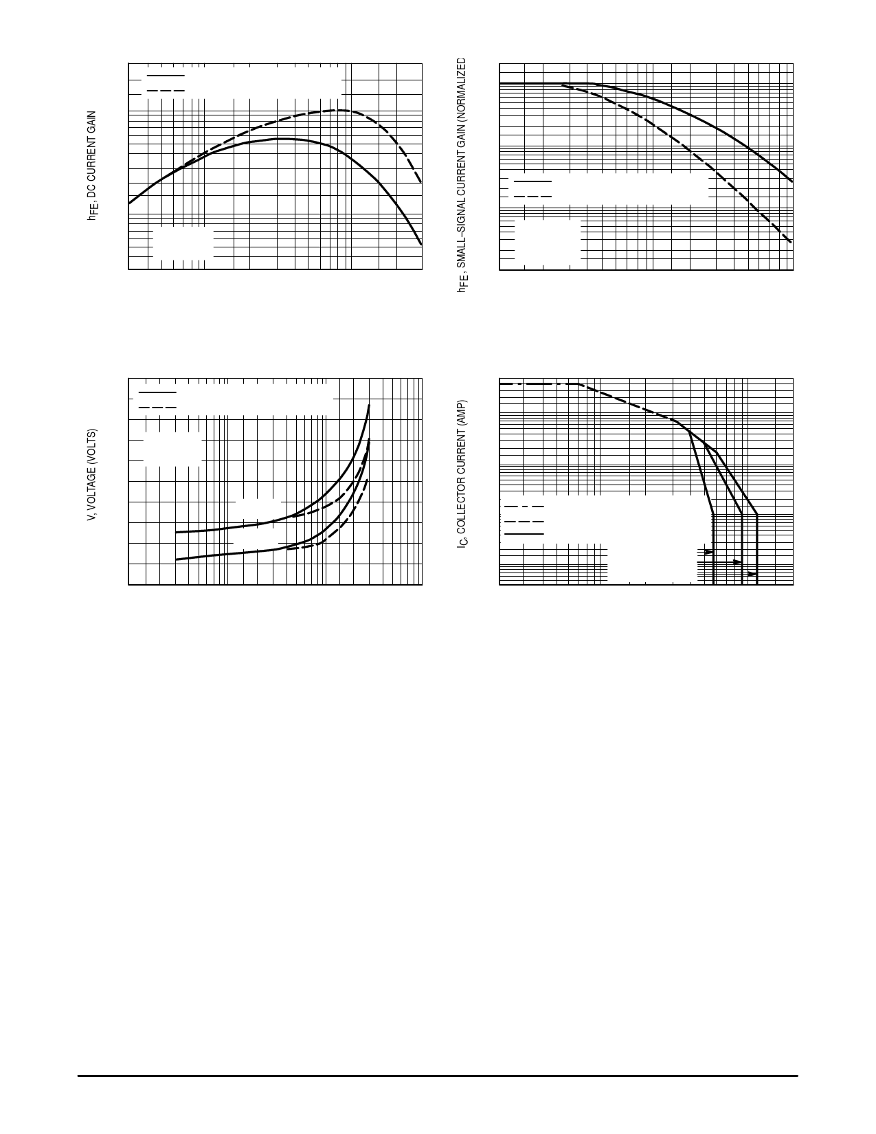
30 k
20 k
PNP MJ11013, MJ11015
NPN MJ11012, MJ11014, MJ11016
10 k
7k
5k
3k
2k
700
500
300
0.3
VCE = 5 Vdc
TJ = 25°C
0.5 0.7 1
2 3 5 7 10
IC, COLLECTOR CURRENT (AMP)
Figure 2. DC Current Gain (1)
MJ11013 MJ11015 MJ11012 MJ11014 MJ11016
2
1
0.5
20 30
0.2
0.1
0.05
0.02
PNP MJ11013, MJ11015
NPN MJ11012, MJ11014, MJ11016
0.01
0.005
10
VCE = 3 Vdc
IC = 10 mAdc
TJ = 25°C
20 30
50 70 100 200 300 500 700 1.0 k
f, FREQUENCY (kHz)
Figure 3. Small–Signal Current Gain
5
PNP MJ11013, MJ11015
NPN MJ11012, MJ11014, MJ11016
4
TJ = 25°C
3 IC/IB = 100
2
VBE(sat)
1
VCE(sat)
0
0.1 0.2
0.5 1 2
5 10 20
IC, COLLECTOR CURRENT (AMP)
Figure 4. “On” Voltages (1)
50 100
50
20
10
5
2
1
0.5
0.2
BONDING WIRE LIMITATION
0.1
0.05
THERMAL LIMITATION @ TC = 25°C
SECOND BREAKDOWN LIMITATION
0.02
MJ11012
0.01
MJ11013, MJ11014
MJ11015, MJ11016
23
5 7 10
20 30 50 70 100 200
VCE, COLLECTOR–EMITTER VOLTAGE (VOLTS)
Figure 5. Active Region DC Safe Operating Area
There are two limitations on the power handling ability of a
transistor average junction temperature and secondary
breakdown. Safe operating area curves indicate IC – VCE lim-
its of the transistor that must be observed for reliable opera-
tions e.g., the transistor must not be subjected to greater
dissipation than the curves indicate.
At high case temperatures, thermal limitations will reduce
the power that can be handled to values less than the limita-
tions imposed by secondary breakdown.
Motorola Bipolar Power Transistor Device Data
3
Share Link: 