HT7727A(2007) 查看數據表(PDF) - Holtek Semiconductor
零件编号
产品描述 (功能)
比赛名单
HT7727A Datasheet PDF : 18 Pages
| |||
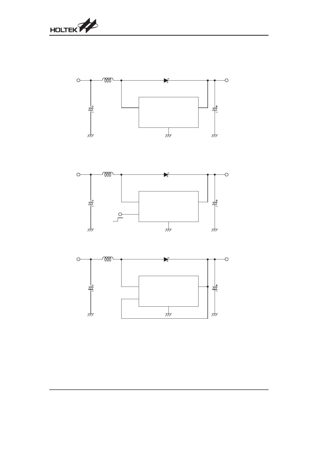
Application Circuits
Without CE Pin
47mH ~100mH
V IN
1N 5817
HT77XXA
V OUT
4 7 m F ( T a n ta lu m )
LX
H T77X X A
VO UT
S e r ie s
GND
With CE Pin
V IN
47mH ~100mH
1N 5817
2 2 m F ( T a n ta lu m )
V OUT
4 7 m F ( T a n ta lu m )
LX
H T77X X A
VO UT
S e r ie s
CE
GND
2 2 m F ( T a n ta lu m )
47mH ~100mH
1N 5817
V IN
V OUT
4 7 m F ( T a n ta lu m )
LX
H T77X X A
VO UT
S e r ie s
CE
GND
2 2 m F ( T a n ta lu m )
Note:
For the SOT-25 package, when CE is pulled low, the internal blocks of the device, such as the reference band
gap, gain block, and all feedback and control circuitry will be switched off. The boost converter¢s output, VOUT,
will be at a value one Schottky diode voltage drop below the input voltage and the LX pin remains in a high im-
pedance condition. The output capacitor and load at VOUT determine the rate at which VOUT decays.
Rev 1.10
8
September 26, 2007
Share Link: 