CD74HC373 查看數據表(PDF) - Philips Electronics
零件编号
产品描述 (功能)
比赛名单
CD74HC373 Datasheet PDF : 8 Pages
| |||
Philips Semiconductors
24-bit bus switch with 12-bit output enables
Product data
CBT16211
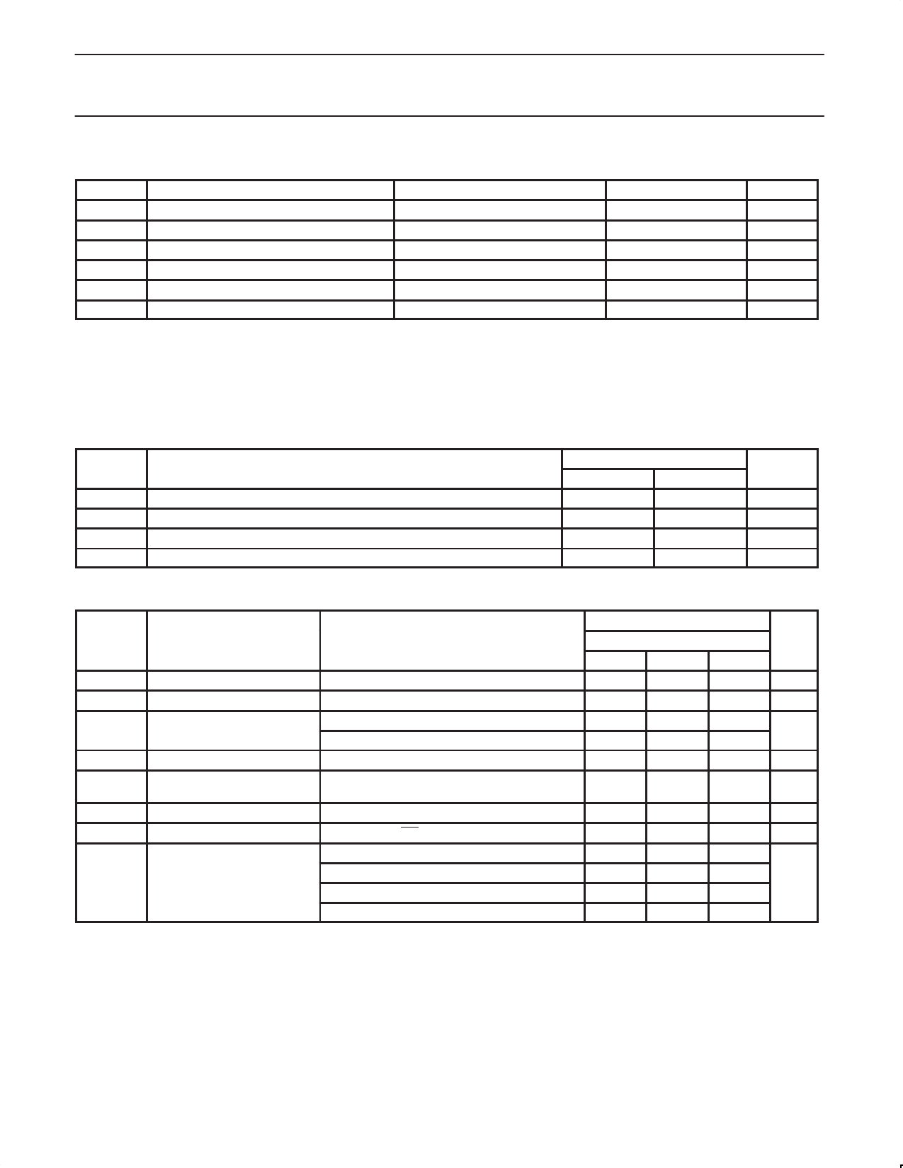
ABSOLUTE MAXIMUM RATINGS1, 2
SYMBOL
PARAMETER
CONDITIONS
RATING
UNIT
VCC
DC supply voltage
–0.5 to +7.0
V
IIK
DC input diode current
VI < 0
–50
mA
VI
DC input voltage3
–0.5 to +7.0
V
VOUT
DC output voltage3
output in Off or High state
–0.5 to +5.5
V
IOUT
DC output current
output in Low state
128
mA
Tstg
Storage temperature range
–65 to 150
°C
NOTES:
1. Stresses beyond those listed may cause permanent damage to the device. These are stress ratings only and functional operation of the
device at these or any other conditions beyond those indicated under “recommended operating conditions” is not implied. Exposure to
absolute-maximum-rated conditions for extended periods may affect device reliability.
2. The performance capability of a high-performance integrated circuit in conjunction with its thermal environment can create junction
temperatures which are detrimental to reliability. The maximum junction temperature of this integrated circuit should not exceed 150 °C.
3. The input and output voltage ratings may be exceeded if the input and output current ratings are observed.
RECOMMENDED OPERATING CONDITIONS
SYMBOL
PARAMETER
VCC
VIH
VIL
Tamb
DC supply voltage
High-level input voltage
Low-level Input voltage
Operating free-air temperature range
LIMITS
Min
Max
4.5
5.5
2.0
—
—
0.8
–40
+85
UNIT
V
V
V
°C
DC ELECTRICAL CHARACTERISTICS
LIMITS
SYMBOL
PARAMETER
TEST CONDITIONS
Tamb = –40 to +85 °C
Min
Typ1
Max
VIK
Input clamp voltage
VCC = 4.5 V; II = –18 mA
—
—
–1.2
VP
Output high pass voltage
VIN = VCC = 5.0 V; IOUT = –100 µA
3.4
3.6
3.9
II
Input leakage current
VCC = 0 V; VI = 5.5 V
VCC = 5.5 V; VI = GND or 5.5 V
—
—
10
—
—
±1
ICC
Quiescent supply current
VCC = 5.5 V; IO = 0, VI = VCC or GND
—
—
3
∆ICC
Additional supply current per
input pin2
VCC = 5.5 V, one input at 3.4 V,
other inputs at VCC or GND
—
—
2.5
CI
Control pins
VI= 3 V or 0
—
4.5
—
CI(OFF) Port OFF capacitance
VO = 3 V or 0, OE = VCC
—
6.9
—
VCC = 4.0 V; V1 = 2.4 V; II = 15 mA
—
14
20
ron3
VCC = 4.5 V; V1 = 0 V; II = 64 mA
VCC = 4.5 V; V1 = 0 V; II = 30 mA
—
5
7
—
5
7
VCC = 4.5 V; V1 = 2.4 V; II = –15 mA
—
8
12
NOTES:
1. All typical values are at VCC = 5 V, Tamb = 25 °C.
2. This is the increase in supply current for each input that is at the specified TTL voltage level rather than VCC or GND.
3. Measured by the voltage drop between the A and the B terminals at the indicated current through the switch.
On-state resistance is determined by the lowest voltage of the two (A or B) terminals.
UNIT
V
V
µA
µA
mA
pF
pF
Ω
2001 Jun 13
4
Share Link: 