MS622424-70 查看數據表(PDF) - Mosel Vitelic, Corp
零件编号
产品描述 (功能)
比赛名单
MS622424-70 Datasheet PDF : 11 Pages
| |||
MOSEL VITELIC
MS622424
Functional Description
MPU Interface
The MPU interface allows the MPU to access the
internal registers and the color map. The
CONFIGSEL0–CONFIGSEL2 bits that are latched
on the falling edge of CEB define the access mode.
The access modes are defined in the table below.
The R/WB pin is also latched on the falling edge of
CEB and indicates a read operation when high and
a write operation when low. These functions are
illustrated in the truth table on the next page.
The RGB0 and RGB1 bits are the two bits of a
modulo 3 counter, which determine which color
(red, green, or blue, in that order) is selected. These
two bits are reset by a write to either the high or low
Address Register. In writes and reads to and from
the color palette, the Address Register is
incremented at the end of the RGB cycle.
In order to perform color pallette read without
asynchronous problems, initialization is required.
This is done by writing a command of
configsel(2:0)=111 before the actual read starts.
Upon finishing the color palette read operation, a
read command of configsel(2:0)=111 should also
be issued to switch MPU Access modes.
During a read from the color palette, the color
data output at POUT0–POUT23 may be disturbed
because the address register will take over
addressing of the color map. To prevent random
color data from being displayed on the screen, the
data at POUT0–POUT23 will be held at the value
defined by the last valid pixel address for the
duration of the read. A read of the color palette
should not be performed while the Write FIFO is not
empty because it may contend with the FIFO to
color map write. It is recommended that FIFO empty
flag status always be checked before issuing color
palette read instructions. If such a contention
occurs, then the color palette read will be disturbed
by the write cycle.
Write FIFO
The Write FIFO stores data and addresses that
are written to the Color Palette Buffer and Address
Registers. The FIFO is emptied by writing the data
to the color map during a blanking period as
indicated by CBLANKB. The host can write up to 64
locations that contain a 13-bit address and a 24-bit
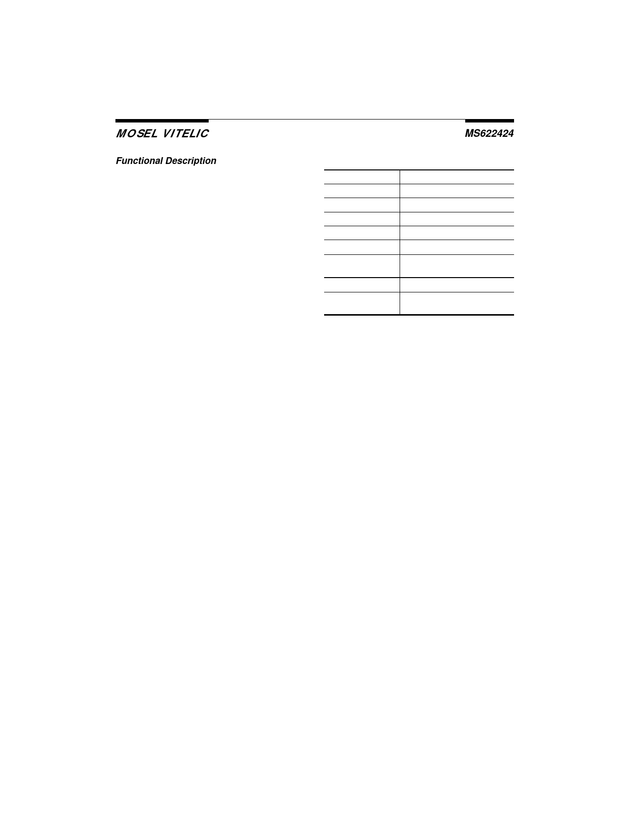
MPU Access Modes
CONFIGSEL<2:0> MODE
000
Address Register low (R/W)
001
Address Register high (R/W)
010
Color Palette Buffer (R/W)
011
Command Register (R/W)
100
Status Register (read only)
101
Color Buffer Register
(read only)
110
Revision register (read only)
111
Color Palette read initialization
(R/W)
color before the FIFO becomes full. When the FIFO
is full the full flag pin (FFB) goes low until at least
one location of the FIFO is transferred to the color
map. If the host attempts to write to the Color
Palette Buffer while the FFB is active, then the
device will transfer 4 locations from the FIFO to the
color map in order to make room for the incoming
data, regardless of the state of CBLANKB. This
process may disturb the data in the pixel stream. To
prevent random color data from being displayed on
the screen while the device performs these 4 writes,
the data at POUT0–POUT23 will be held at the
value defined by the last valid pixel address. When
Pixel clock is much slower than 70 MHz, the
operating frequency of MPU should also be slowed
down accordingly in order to maintain the
synchronization of FIFO operations
Color Buffer Register
The Color Buffer Register stores the red and
green data that is written to the Color Palette Buffer.
Thus if a complete red, green, blue write cycle is not
completed (register data is not transferred to the
Write FIFO), then the host can recover the red and
green data it has written by reading the red and
green Color Buffer Registers.
The host can recover the red and green data by
first writing to the address register to reset the RGB
counter. Then the red and green data can be
recovered in two consecutive reads of the Color
Buffer Register.
MS622424 Rev. 1.0 January 1995
8-2
Share Link: 