78Q8392L 查看數據表(PDF) - TDK Corporation
零件编号
产品描述 (功能)
比赛名单
78Q8392L Datasheet PDF : 12 Pages
| |||
78Q8392L
Low Power Ethernet
Coaxial Transceiver
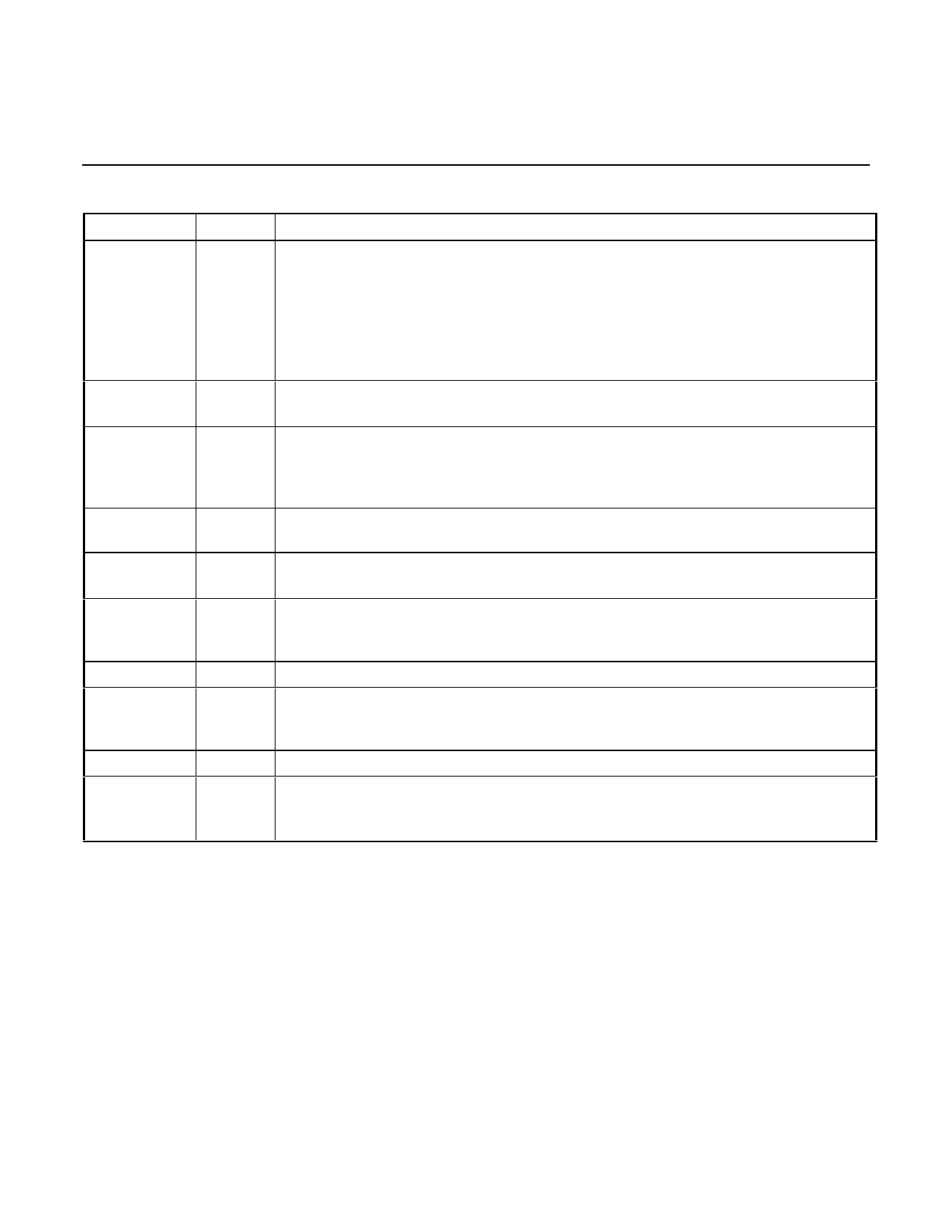
PIN DESCRIPTION
NAME
TYPE DESCRIPTION
CD+*/CD-
O
Collision Output. Balanced differential line driver outputs from the collision detect
circuitry. The 10 MHz signal from the internal oscillator is transferred to these outputs
in the event of collision, excessive transmission (jabber), or during CD Heartbeat
condition. These outputs are open emitters; pulldown resistors to VEE are required.
When operating into a 78Ω transmission line, these resistors should be 510Ω. In
Cheapernet applications, where the 78Ω drop cable is not used, higher resistor
values (up to 1.5k) may be used to save power.
RX+*/RX-
O
Receive Output. Balanced differential line driver outputs from the Receiver. These
outputs also require 510Ω pulldown resistors.
TX+*/TX-
I
Transmit Input. Balanced differential line receiver inputs to the Transmitter. The
common mode voltage for these inputs is determined internally and must not be
externally established. Signals meeting Transmitter squelch requirements are
waveshaped and output at TXO.
HBE
I
Heartbeat Enable. This input enables CD Heartbeat when grounded or left opened,
disables it when connected to VEE.
RR+/RR-
I
External Resistor. A fixed 1 kΩ 1% resistor connected between these pins
establishes internal operating currents.
RXI
I
Receive Input. Connects directly to the coaxial cable. Signals meeting Receiver
squelch requirements are equalized for inter-symbol distortion, amplified, and output
at RX+ and RX- pin.
TXO
O
Transmit Output. Connects via an isolation diode to the coaxial cable.
CDS
I
Collision Detect Sense. Ground sense connection for the collision detect circuit. This
pin should be connected separately to the shield to avoid ground drops from altering
the receive mode collision threshold.
GND
S
Positive Supply Pin.
VEE
S
Negative Supply Pins. These pins should be connected to a large metal frame area
on the PC board to handle heat dissipation, and bypassed to the GND pin with a 0.1
µF capacitor as close to the package as possible.
*IEEE names for CD± = CI±, RX± = DI±, TX± = DO±
Notes: Pin type: I-input; O-output; S-power supply
4
Share Link: 