DM74ALS640A 查看數據表(PDF) - Fairchild Semiconductor
零件编号
产品描述 (功能)
比赛名单
DM74ALS640A Datasheet PDF : 4 Pages
| |||
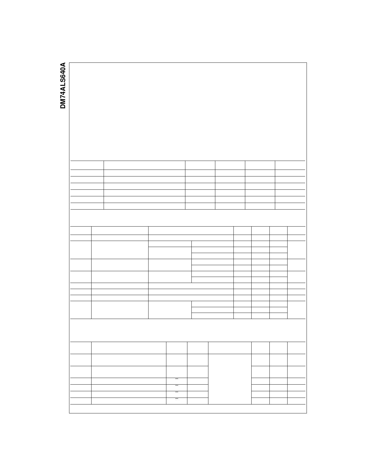
Absolute Maximum Ratings(Note 1)
Supply Voltage
Input Voltage
Control Inputs
I/O ports
Operating Free Air Temperature Range
Storage Temperature Range
Typical θJA
N Package
M Package
7V
7V
5.5V
0°C to +70°C
−65°C to +150°C
53.0°C/W
72.0°C/W
Note 1: The “Absolute Maximum Ratings” are those values beyond which
the safety of the device cannot be guaranteed. The device should not be
operated at these limits. The parametric values defined in the Electrical
Characteristics tables are not guaranteed at the absolute maximum ratings.
The “Recommended Operating Conditions” table will define the conditions
for actual device operation.
Recommended Operating Conditions
Symbol
Parameter
Min
Typ
VCC
Supply Voltage
4.5
5
VIH
HIGH Level Input Voltage
2
VIL
LOW Level Input Voltage
IOH
HIGH Level Output Current
IOL
LOW Level Output Current
TA
Operating Free Air Temperature Range
0
Electrical Characteristics
Over Recommended Free Air Temperature Range
Symbol
Parameter
Test Conditions
VIC
Input Clamp Voltage
VOH
HIGH Level
Output Voltage
VOL
LOW Level
Output Voltage
II
Input Current at Maximum
Input Voltage
IIH
HIGH Level Input Current
IIL
LOW Level Input Current
IO
Output Drive Current
ICC
Supply Current
VCC = Min, II = −18 mA
VCC = 4.5 to 5.5V
IOH = −0.4 mA
VCC = Min
IOH = − 3 mA
IOH = Max
VCC = Min
IOL = 12 mA
IOL = 24 mA
VCC = Max.
I/O Ports, VI = 5.5V
Control Inputs, VI = 7V
VCC = Max, VI = 2.7V (Note 2)
VCC = Max, VI = 0.4V (Note 2)
VCC = Max, VO = 2.25V
VCC = Max
Outputs HIGH
Outputs LOW
Outputs Disabled
Note 2: For I/O ports, IIH and IILparameters include the 3-STATE output current (IOZL and IOZH).
Min
VCC − 2
2.4
2
−30
Switching Characteristics
Over Recommended Operating Free Air Temperature Range
Symbol
Parameter
From
(Input)
tPLH
Propagation Delay Time
LOW-to-HIGH Level Output
A or B
tPHL
Propagation Delay Time
HIGH-to-LOW Level Output
A or B
tPZH
Output Enable Time to HIGH Level Output
G
tPZL
Output Enable Time to LOW Level Output
G
tPHZ
Output Disable Time from HIGH Level Output
G
tPLZ
Output Disable Time from LOW Level Output
G
To
(Output)
B or A
B or A
A or B
A or B
A or B
A or B
Conditions
VCC = 4.5 to 5.5V,
CL = 50 pF,
R1 = R2 = 500Ω
Max
5.5
0.8
−15
24
70
Typ
2.9
0.25
0.35
19
23
17
Min
1
1
4
5
1
3
Units
V
V
V
mA
mA
°C
Max
Units
−1.5
V
V
0.4
V
0.5
100
µA
100
20
µA
−100
µA
−112
mA
45
55
mA
50
Max
Units
11
ns
10
ns
21
ns
24
ns
10
ns
15
ns
www.fairchildsemi.com
2
Share Link: 