ESD7481MUT5G(2012) 查看數據表(PDF) - ON Semiconductor
零件编号
产品描述 (功能)
比赛名单
ESD7481MUT5G Datasheet PDF : 5 Pages
| |||
ESD7481MUT5G
ELECTRICAL CHARACTERISTICS
(TA = 25°C unless otherwise noted)
Symbol
Parameter
IPP
Maximum Reverse Peak Pulse Current
VC
Clamping Voltage @ IPP
VRWM Working Peak Reverse Voltage
IR
Maximum Reverse Leakage Current @ VRWM
VBR
Breakdown Voltage @ IT
IT
Test Current
*See Application Note AND8308/D for detailed explanations of
datasheet parameters.
I
IPP
VC VBR VRWM IIRT
IIRT
VRWM VBR VC V
IPP
Bi−Directional TVS
ELECTRICAL CHARACTERISTICS (TA = 25°C unless otherwise specified)
Parameter
Symbol
Conditions
Reverse Working Voltage
Breakdown Voltage (Note 2)
Reverse Leakage Current
Clamping Voltage (Note 3)
Clamping Voltage (Note 3)
ESD Clamping Voltage
Junction Capacitance
Dynamic Resistance
Insertion Loss
VRWM
VBR
IR
VC
VC
VC
CJ
RDYN
IT = 1 mA
VRWM = 3.3 V
IPP = 1 A
IPP = 3 A
Per IEC61000−4−2
VR = 0 V, f = 1 Mhz
VR = 0 V, f < 1 GHz
TLP Pulse
f = 1 Mhz
f = 8.5 GHz
2. Breakdown voltage is tested from pin 1 to 2 and pin 2 to 1.
3. Non−repetitive current pulse at TA = 25°C, per IEC61000−4−5 waveform.
Min
Typ
Max Unit
3.3
V
6.0
V
< 1.0
50
nA
10
V
12
V
See Figures 1 and 2
0.25
0.40
pF
0.15
0.30
0.60
W
0.030
dB
0.234
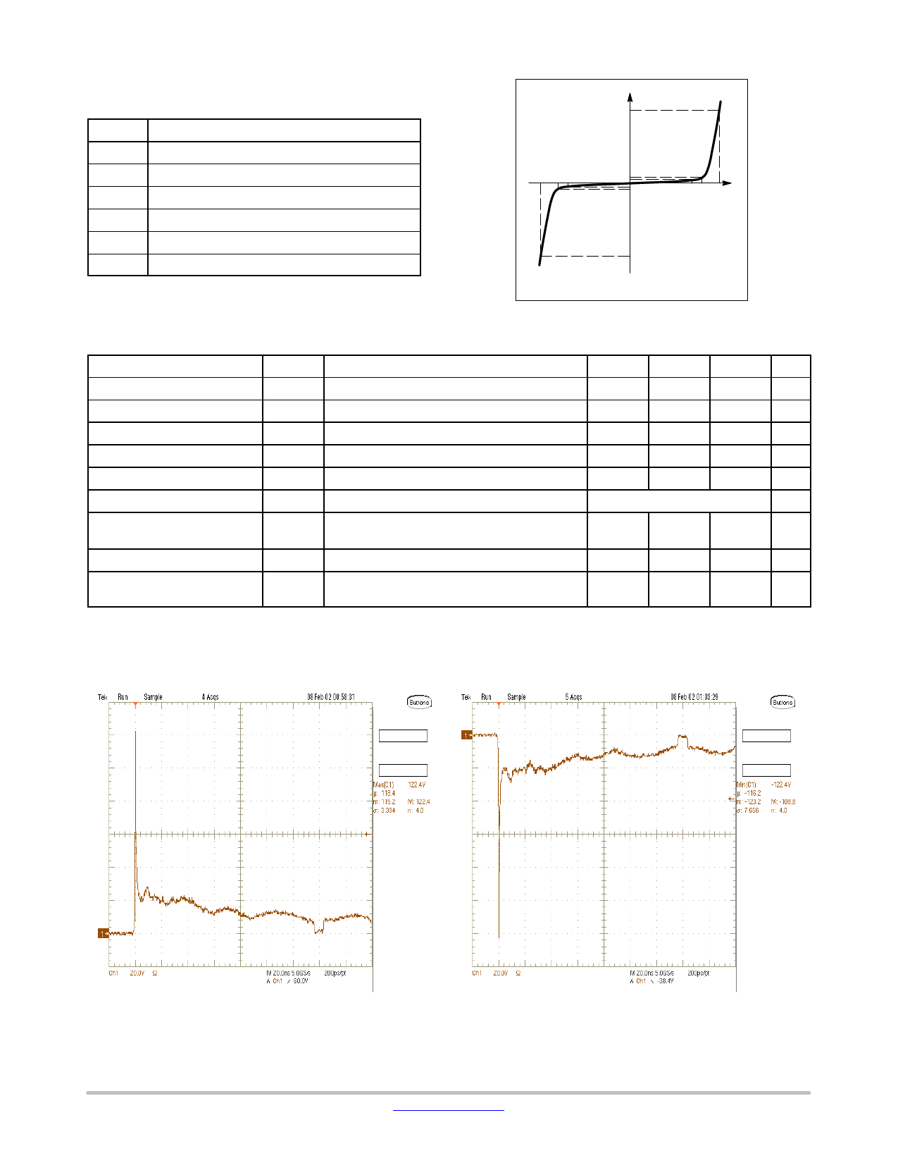
Figure 1. ESD Clamping Voltage Screenshot
Positive 8 kV Contact per IEC61000−4−2
Figure 2. ESD Clamping Voltage Screenshot
Negative 8 kV Contact per IEC61000−4−2
http://onsemi.com
2
Share Link: 