74HC367 查看數據表(PDF) - NXP Semiconductors.
零件编号
产品描述 (功能)
比赛名单
74HC367 Datasheet PDF : 18 Pages
| |||
Nexperia
74HC367; 74HCT367
Hex buffer/line driver; 3-state
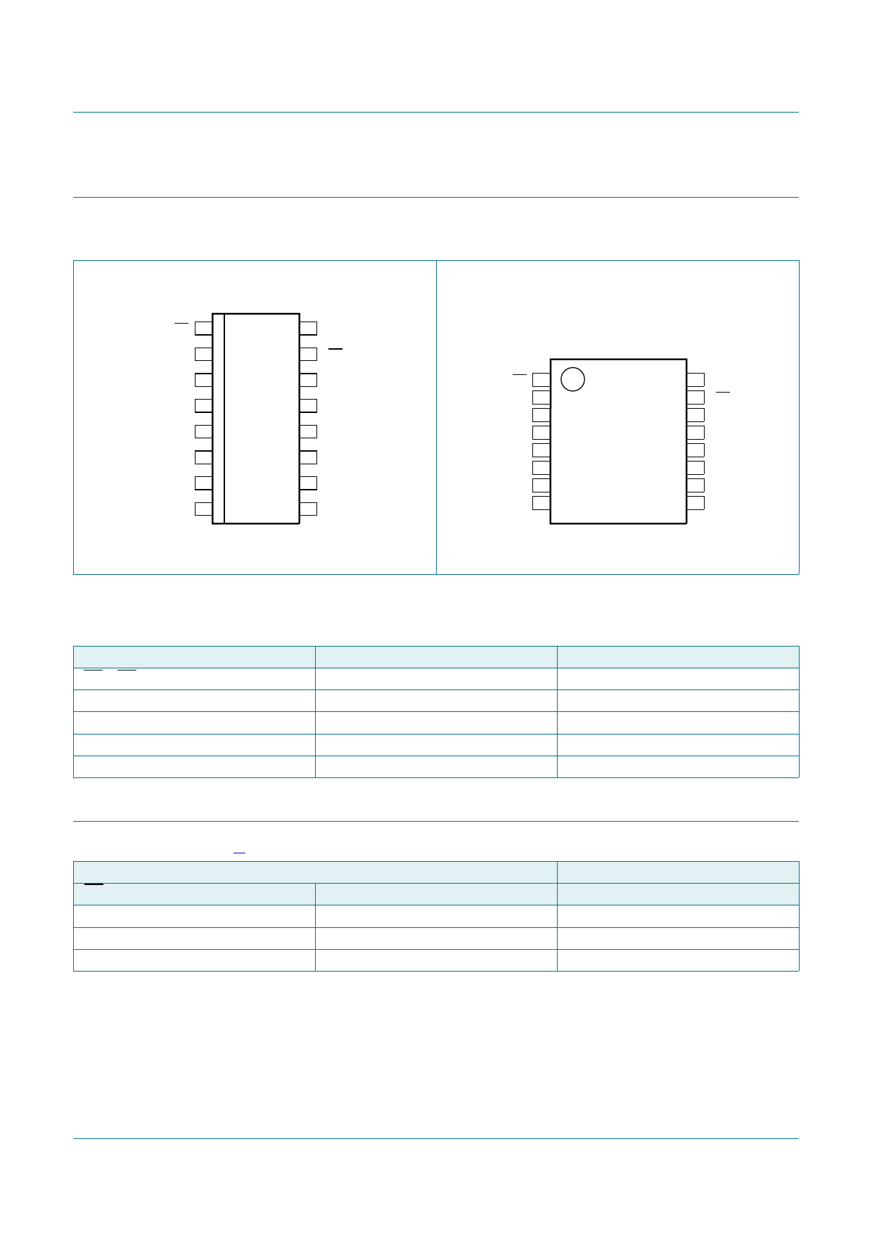
5. Pinning information
5.1 Pinning
+&
+&7
2(
$
<
$
<
$
<
*1'
9&&
2(
$
<
$
<
$
<
DDD
Fig 4. Pin configuration SO16
+&
+&7
2(
$
<
$
<
$
<
*1'
9&&
2(
$
<
$
<
$
<
DDD
Fig 5. Pin configuration (T)SSOP16
5.2 Pin description
Table 2. Pin description
Symbol
1OE, 2OE
1A, 2A, 3A, 4A, 5A, 6A
1Y, 2Y, 3Y, 4Y, 5Y, 6Y
GND
VCC
Pin
1, 15
2, 4, 6, 10, 12, 14
3, 5, 7, 9, 11, 13
8
16
6. Functional description
Description
output enable input (active LOW)
data input
bus output
ground (0 V)
supply voltage
Table 3. Function table[1]
Input
nOE
nA
L
L
L
H
H
X
Output
nY
L
H
Z
[1] H = HIGH voltage level; L = LOW voltage level; X = don’t care; Z = high-impedance OFF-state.
74HC_HCT367
Product data sheet
All information provided in this document is subject to legal disclaimers.
Rev. 3 — 17 October 2016
© Nexperia B.V. 2017. All rights reserved
4 of 18
Share Link: 