74LVC544A 查看數據表(PDF) - NXP Semiconductors.
零件编号
产品描述 (功能)
比赛名单
74LVC544A Datasheet PDF : 19 Pages
| |||
NXP Semiconductors
74LVC544A
Octal D-type registered transceiver; inverting; 3-state
Table 7. Dynamic characteristics …continued
Voltages are referenced to GND (ground = 0 V). For test circuit see Figure 9.
Symbol Parameter Conditions
40 C to +85 C
Min Typ[1] Max
tsk(o)
output skew VCC = 3.0 V to 3.6 V
time
[3]
-
-
1.0
CPD
power
VI = GND to VCC
dissipation
capacitance
VCC = 1.65 V to 1.95 V
VCC = 2.3 V to 2.7 V
[4]
-
8.1
-
-
11.8
-
VCC = 3.0 V to 3.6 V
-
15.1
-
40 C to +125 C Unit
Min
Max
-
1.5 ns
-
- pF
-
- pF
-
- pF
[1] Typical values are measured at Tamb = 25 C and VCC = 1.2 V, 1.8 V, 2.5 V, 2.7 V and 3.3 V respectively.
[2] tpd is the same as tPLH and tPHL.
ten is the same as tPZL and tPZH.
tdis is the same as tPLZ and tPHZ.
[3] Skew between any two outputs of the same package switching in the same direction. This parameter is guaranteed by design.
[4] CPD is used to determine the dynamic power dissipation (PD in W).
PD = CPD VCC2 fi N + (CL VCC2 fo) where:
fi = input frequency in MHz; fo = output frequency in MHz
CL = output load capacitance in pF
VCC = supply voltage in Volts
N = number of inputs switching
(CL VCC2 fo) = sum of the outputs
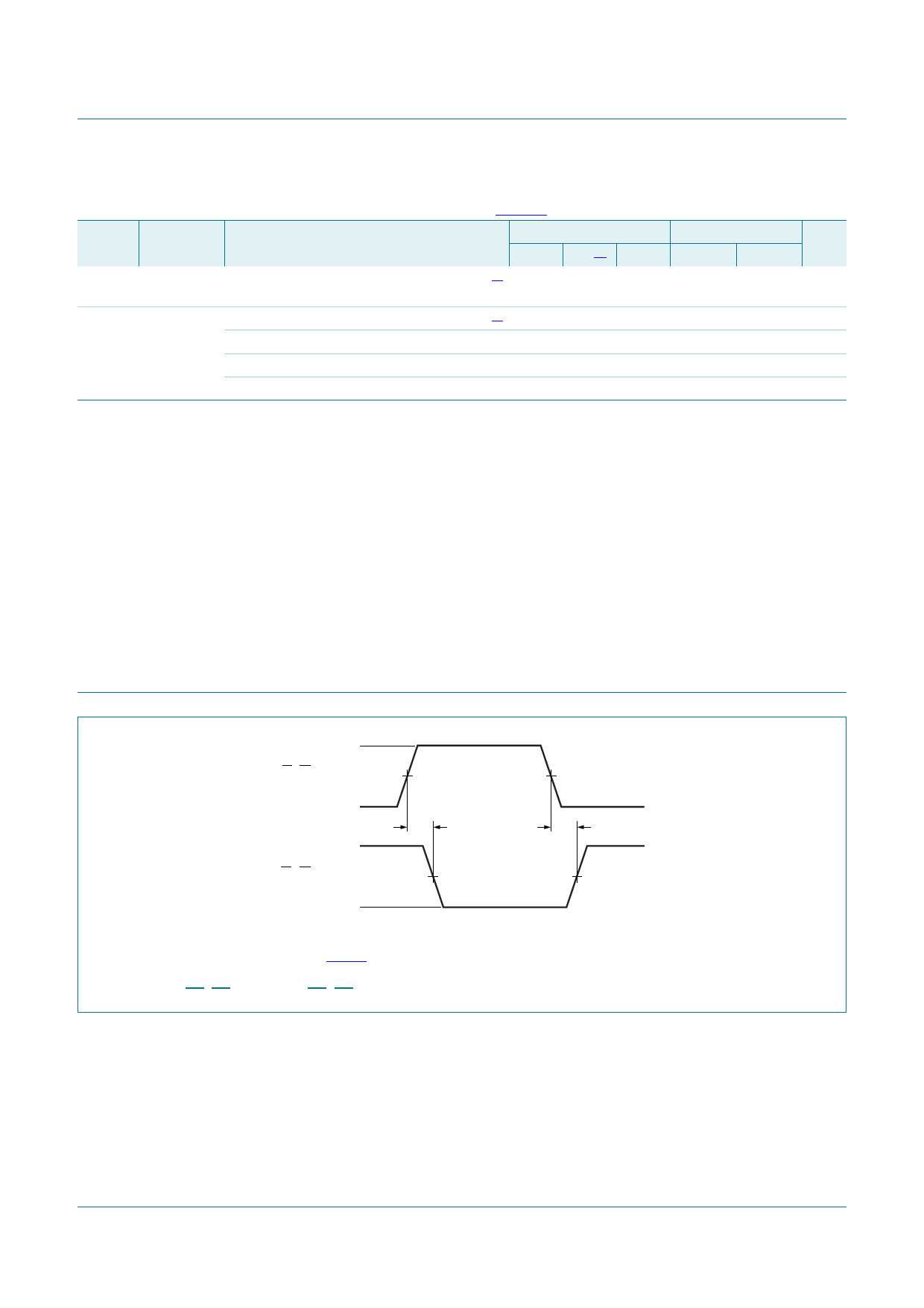
11. Waveforms
VI
An, Bn input
GND
VOH
Bn, An output
VOL
VM
tPHL
VM
tPLH
001aaa785
Fig 5.
Measurement points are given in Table 8.
VOL and VOH are typical output voltage levels that occur with the output load.
Input (An, Bn) to output (Bn, An) propagation delays
74LVC544A
Product data sheet
All information provided in this document is subject to legal disclaimers.
Rev. 4 — 18 December 2012
© NXP B.V. 2012. All rights reserved.
9 of 19
Share Link: 