D78F9189CT 查看數據表(PDF) - NEC => Renesas Technology
零件编号
产品描述 (功能)
比赛名单
D78F9189CT Datasheet PDF : 247 Pages
| |||
CHAPTER 2 PIN FUNCTIONS
2.3 Pin Input/Output Circuits and Recommended Connection of Unused Pins
The input/output circuit type of each pin and recommended connection of unused pins are shown in Table 2-1.
For the input/output circuit configuration of each type, refer to Figure 2-1.
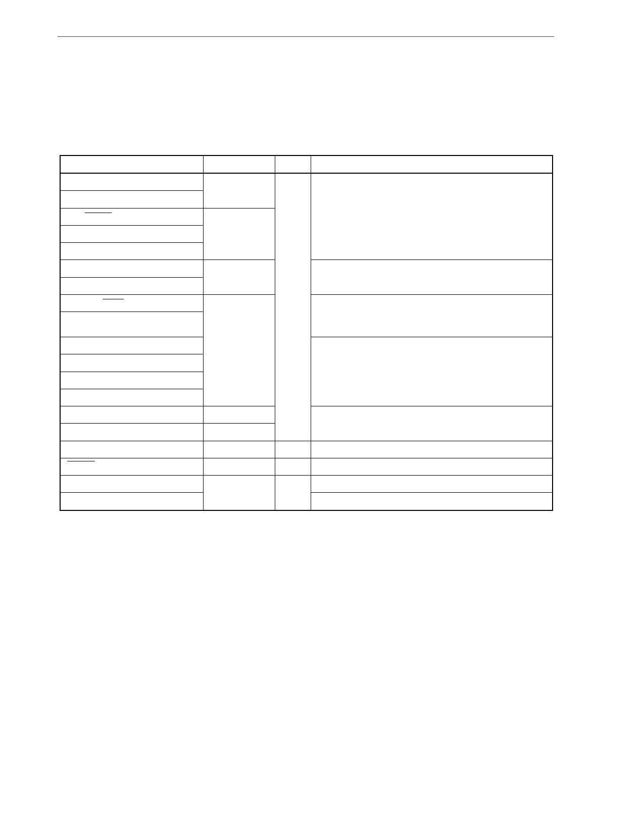
Table 2-1. Types of Input/Output Circuits for Each Pin and Recommended Connection of Unused Pins
Pin Name
P00 to P04
P10, P11
P20/SCK20/ASCK20
P21/SO20/TxD20
P22/SI20/RxD20
P23
P24
P25/TI80/SS20
P26/TO80
I/O Circuit Type
5-H
8-C
13-X
8-C
P30/INTP0/TI81/CPT90
P31/INTP1/TO81
P32/INTP2/TO90
P33/INTP3/TO82/BZO90
P50 to P53 (mask ROM version)
P50 to P53 (flash memory version)
P60/ANI0 to P63/ANI3
RESET
IC0 (mask ROM version)
VPP (flash memory version)
13-U
13-T
9-C
2
−
I/O
I/O
Input
Input
−
Recommended Connection of Unused Pins
Input: Independently connect to VDD or VSS via a resistor.
Output: Leave open.
Input: Independently connect to VDD via a resistor.
Output: Leave open.
Input: Independently connect to VDD or VSS
via a resistor.
Output: Leave open.
Input: Independently connect to VSS via a resistor.
Output: Leave open.
Input: Independently connect to VDD via a resistor.
Output: Leave open.
Connect directly to VDD or VSS.
−
Connect directly to VSS.
Connect directly to VSS.
28
User’s Manual 2nd edition
Share Link: 