SIA811ADJ-T1-GE3 查看數據表(PDF) - Vishay Semiconductors
零件编号
产品描述 (功能)
比赛名单
SIA811ADJ-T1-GE3 Datasheet PDF : 12 Pages
| |||
www.vishay.com
SiA811ADJ
Vishay Siliconix
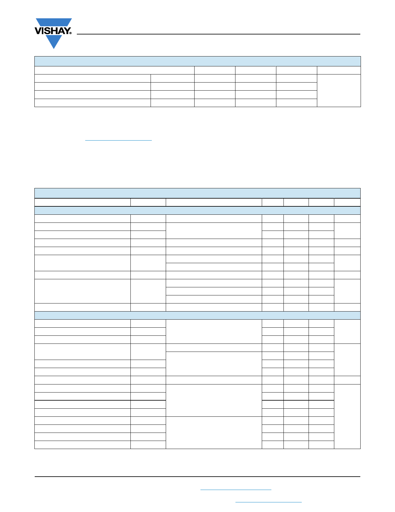
THERMAL RESISTANCE RATINGS
PARAMETER
Maximum junction-to-ambient (MOSFET) b, f
Maximum junction-to-case (drain) (MOSFET)
Maximum junction-to-ambient (Schottky) b, f
Maximum junction-to-case (drain) (Schottky)
t 5 s
Steady state
t5s
Steady state
SYMBOL
RthJA
RthJC
RthJA
RthJC
TYPICAL
55
15
62
15
MAXIMUM
70
19
76
18.5
UNIT
°C/W
Notes
a. Package limited
b. Surface mounted on 1" x 1" FR4 board
c. t = 10 s
d. See solder profile (www.vishay.com/ppg?73257). The PowerPAK SC-70 is a leadless package. The end of the lead terminal is exposed
copper (not plated) as a result of the singulation process in manufacturing. A solder fillet at the exposed copper tip cannot be guaranteed and
is not required to ensure adequate bottom side solder interconnection
e. Rework conditions: manual soldering with a soldering iron is not recommended for leadless components
f. Maximum under steady state conditions is 110 °C/W
SPECIFICATIONS (TJ = 25 °C, unless otherwise noted)
PARAMETER
SYMBOL
TEST CONDITIONS
Static
Drain-source breakdown voltage
VDS temperature coefficient
VGS(th) temperature coefficient
Gate-source threshold voltage
Gate-source leakage
Zero gate voltage drain current
On-state drain current a
Drain-source on-state resistance a
Forward transconductance a
Dynamic b
VDS
VDS/TJ
VGS(th)/TJ
VGS(th)
IGSS
IDSS
ID(on)
RDS(on)
gfs
VGS = 0 V, ID = -250 μA
ID = -250 μA
VDS = VGS, ID = -250 μA
VDS = 0 V, VGS = ± 8 V
VDS = -20 V, VGS = 0 V
VDS = -20 V, VGS = 0 V, TJ = 55 °C
VDS 5 V, VGS = -4.5 V
VGS = -4.5 V, ID = -2.8 A
VGS = -2.5 V, ID = -2.3 A
VGS = -1.8 V, ID = -0.54 A
VDS = -10 V, ID = -2.8 A
Input capacitance
Output capacitance
Reverse transfer capacitance
Total gate charge
Ciss
Coss
Crss
Qg
VDS = -10 V, VGS = 0 V, f = 1 MHz
VDS = -10 V, VGS = -8 V, ID = -3.5 A
Gate-source charge
Gate-drain charge
Gate resistance
Turn-on delay time
Rise time
Turn-off delay time
Fall time
Turn-on delay time
Rise time
Turn-off delay time
Fall time
Qgs
Qgd
Rg
td(on)
tr
td(off)
tf
td(on)
tr
td(off)
tf
VDS = -10 V, VGS = -4.5 V, ID = -3.5 A
f = 1 MHz
VDD = -10 V, RL = 2.85
ID -3.5 A, VGEN = -4.5 V, Rg = 1
VDD = -10 V, RL = 2.85
ID -3.5 A, VGEN = -8 V, Rg = 1
MIN.
-20
-
-
-0.4
-
-
-
-8
-
-
-
-
-
-
-
-
-
-
-
-
-
-
-
-
-
-
-
-
TYP.
-
-19
2.4
-
-
-
-
-
0.096
0.126
0.165
7
345
65
50
8.4
4.9
0.75
1.2
6
15
45
20
10
5
10
20
10
MAX.
-
-
-
-1
± 100
-1
-10
-
0.116
0.155
0.205
-
-
-
-
13
7.4
-
-
-
25
70
30
15
10
15
30
15
UNIT
V
mV/°C
V
nA
μA
A
S
pF
nC
ns
S-82482-Rev. A, 13-Oct-08
2
Document Number: 68955
For technical questions, contact: pmostechsupport@vishay.com
THIS DOCUMENT IS SUBJECT TO CHANGE WITHOUT NOTICE. THE PRODUCTS DESCRIBED HEREIN AND THIS DOCUMENT
ARE SUBJECT TO SPECIFIC DISCLAIMERS, SET FORTH AT www.vishay.com/doc?91000
Share Link: 