AN6783 查看數據表(PDF) - Panasonic Corporation
零件编号
产品描述 (功能)
比赛名单
AN6783 Datasheet PDF : 9 Pages
| |||
AN6783S
ICs for Timer
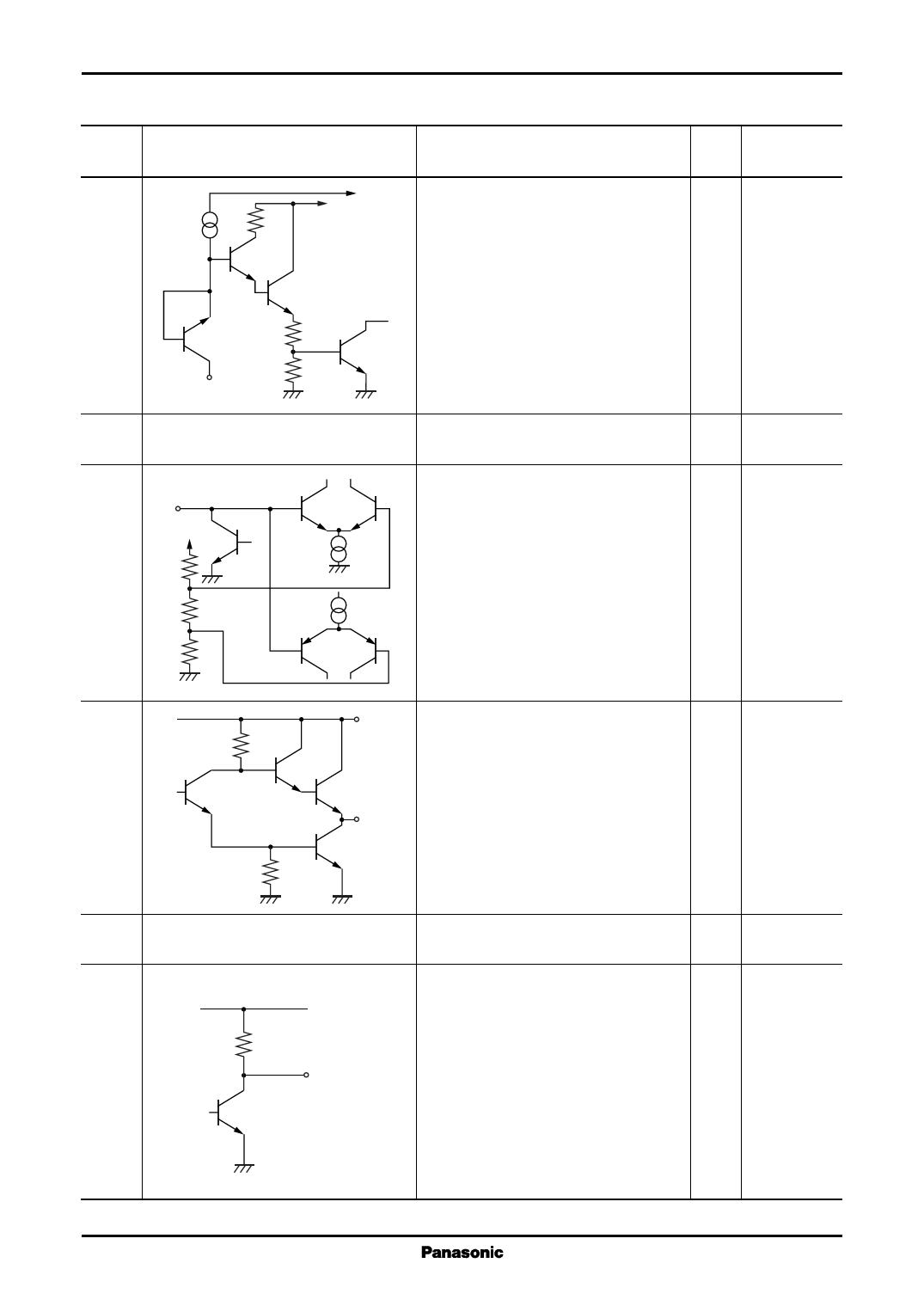
s Terminal Equivalent Circuits (continued)
Pin No.
Equivalent circuit
Description
I/O
3
Reset
VS VCC
Reset :
I
Reset input terminal.
F.F. is reset when the terminal becomes
low-level and is set in the initial state.
When not used, the terminal should be
open or connected to VCC .
The reset is applied by rising VCC from a
voltage below 0.8 V (power-on reset
function).
DC
voltage
4
5
CR
VS
GND :
Grounding terminal.
CR :
C and R connection terminal.
The oscillation period is determined by
an external resistor and capacitor.
When applying a pulse to this terminal
from the outside, the voltage should be
within the range of 0 V to 3 V.
0V
0.7 V to 1.8 V
6
VCC
Out :
O High-level
Output terminal.
VCC −1.4 V
A frequency which is 1/32768 of the
oscillation frequency is outputted.
Low-lebel
Use with an output current within ±10
Out
mA.
< 0.4 V
7
8
VCC
RA = 10 kΩ to 40 kΩ
Mon.
VCC :
Supply voltage terminal.
Mon. :
O
Oscillation frequency monitor terminal.
The output is given from the first stage
of F.F. and a frequency which is 1/2 of
the oscillation frequency fOSC is output-
ted. If not used, the terminal should be
open. This terminal is provided for con-
necting probe such as oscilloscope. Use
it with an output current under 100 µA.
High-level
VCC
Low-level
< 0.4 V
4
Share Link: 