IPD090N03LGE8177 查看數據表(PDF) - Infineon Technologies
零件编号
产品描述 (功能)
比赛名单
IPD090N03LGE8177 Datasheet PDF : 9 Pages
| |||
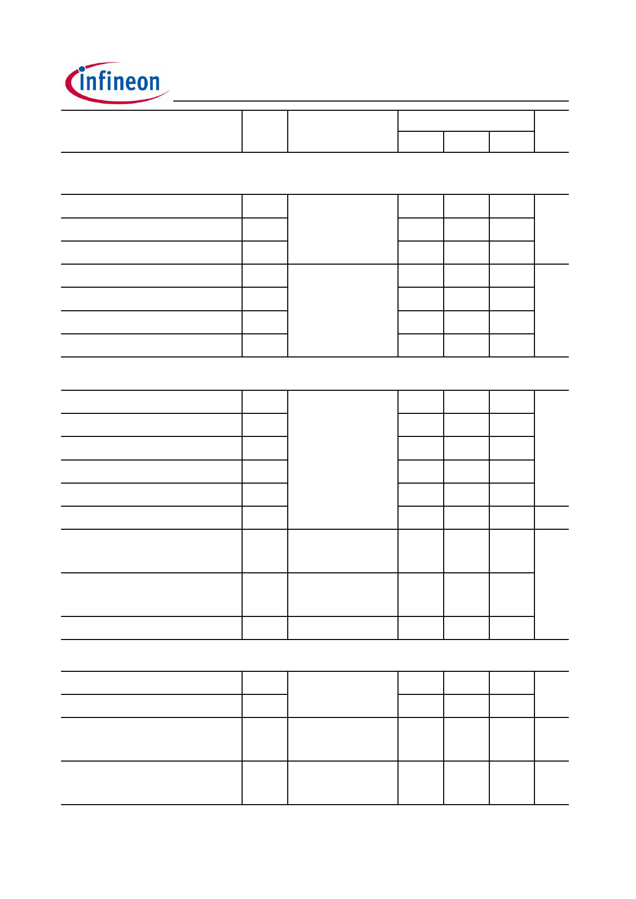
Parameter
Symbol Conditions
IPD090N03L G E8177
min.
Values
typ.
Unit
max.
Dynamic characteristics
Input capacitance
Output capacitance
Reverse transfer capacitance
Turn-on delay time
Rise time
Turn-off delay time
Fall time
C iss
-
C oss
V GS=0 V, V DS=15 V,
f =1 MHz
-
Crss
-
t d(on)
-
tr
V DD=15 V, V GS=10 V,
-
t d(off)
I D=30 A, R G,ext=1.6 W
-
tf
-
Gate Charge Characteristics6)
Gate to source charge
Gate charge at threshold
Gate to drain charge
Switching charge
Gate charge total
Gate plateau voltage
Gate charge total
Gate charge total, sync. FET
Output charge
Q gs
-
Q g(th)
-
Q gd
V DD=15 V, I D=30 A,
-
Q sw
V GS=0 to 4.5 V
-
Qg
-
V plateau
-
Qg
V DD=15 V, I D=30 A,
V GS=0 to 10 V
-
Q g(sync)
V DS=0.1 V,
V GS=0 to 4.5 V
-
Q oss
V DD=15 V, V GS=0 V
-
Reverse Diode
Diode continuous forward current I S
-
T C=25 °C
Diode pulse current
I S,pulse
-
Diode forward voltage
V SD
V GS=0 V, I F=30 A,
T j=25 °C
-
Reverse recovery charge
Q rr
V R=15 V, I F=I S,
di F/dt =400 A/µs
-
6) See figure 16 for gate charge parameter definition
Rev. 2.0
page 3
1200
460
24
4.0
3
15
2.6
1600 pF
610
-
- ns
-
-
-
4.0
- nC
1.8
-
1.8
-
3.8
-
7.2
9.6
3.4
-V
15
-
6.3
8.3 nC
12
-
-
37 A
-
280
0.93
1.1 V
-
10 nC
2014-01-14
Share Link: 