TDA7469A 查看數據表(PDF) - STMicroelectronics
零件编号
产品描述 (功能)
比赛名单
TDA7469A Datasheet PDF : 17 Pages
| |||
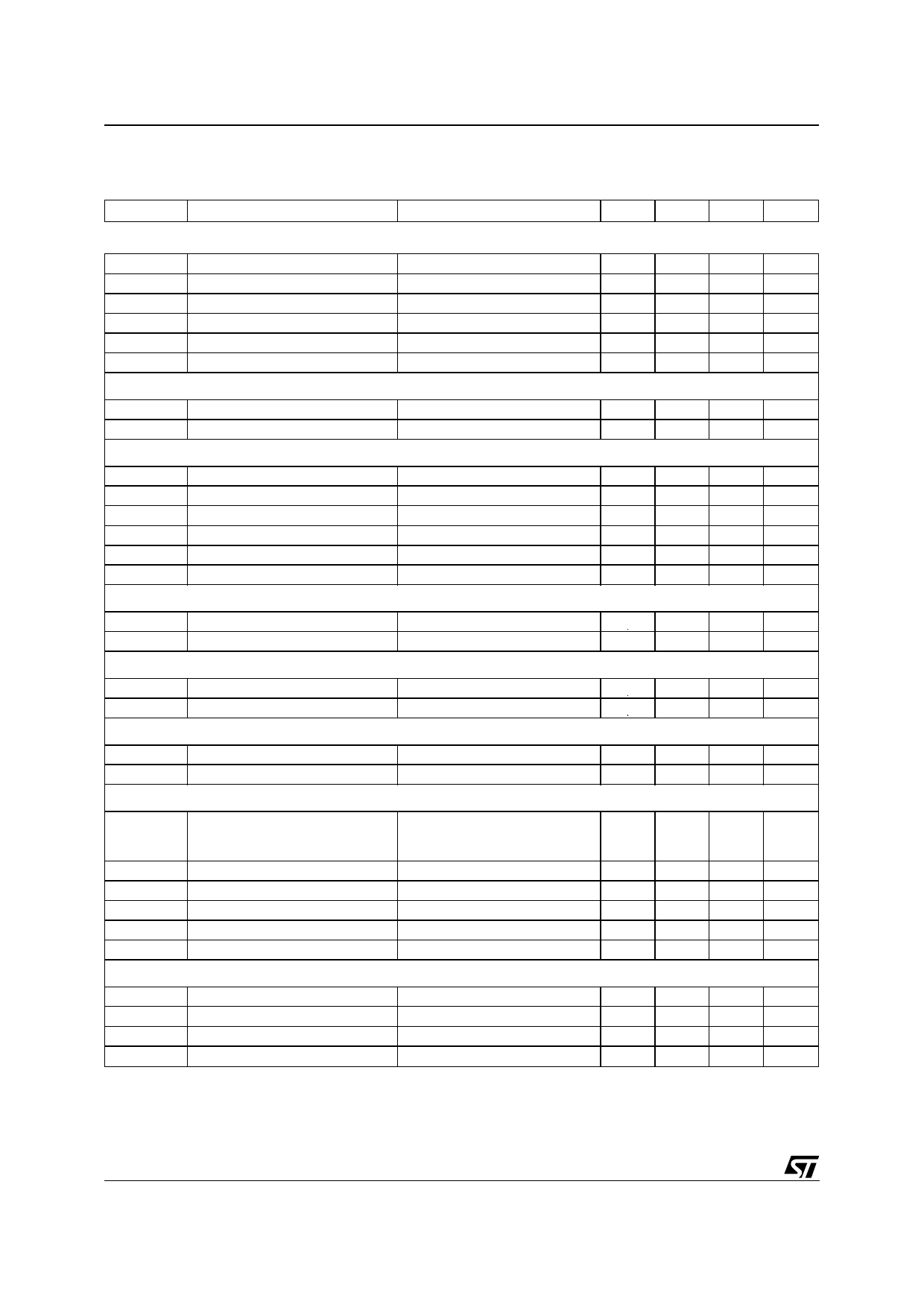
TDA7469
ELECTRICAL CHARACTERISTICS (refer to the test circuit Tamb = 25°C, VS =2.4V, all controls flat
(G = 0dB), f = 1KHz, unless otherwise specified)
Symbol
SUPPLY
Parameter
Test Condition
Min. Typ. Max. Unit
VS
Supply Voltage
VPS
Supply Voltage
ISQ
Supply Current
IPSQ
Quiscent Current
IS
IPS
INPUT STAGE
RIN
Input Resistance
AIN
Input Attenuation Range
Po = 0.5mW +0.5mW
Po = 0.5mW +0.5mW
1.8
2.4
5.0
V
1.5
2.4
5.0
V
10
µA
1
µA
8
mA
15
mA
35
50
65
KΩ
0
6
dB
VOLUME CONTROL
CRANGE Control Range
AMAX
Max. Attenuation
ASTEP
Step Resolution
GMAX
Max. Gain
Gstep Step Resolution
R1
Muxout Load Resistence
-63
6
dB
61
63
65
dB
0.5
1
1.5
dB
6
dB
2
dB
10
KΩ
BASS CONTROL
Gb
Control Range
RB
Internal Feedback Resistance
TREBLE CONTROL
Gt
Control Range
Rt
Internal Resistance
Max. Boost/on
Max. Boost
14
dB
75.6 100.8 126 KΩ
12
dB
25
KΩ
HEADPHONE OUTPUTS
Gout
Output Gain
Pomax Max Output Power
THD = 10%
0
dB
5
8
mW
GENERAL
ENO
Output Noise
THD
SC
RR1
RR2
Distortion
Channel Separation Left/Right
Ripple Rejection
Ripple Rejection
Total Tracking Error
Outout Muted
All gains = 0dB;
BW = 20Hz to 20KHz flat
Av = 0, Vin = 0.1Vrms
VS, f = 100Hz
PVS, f = 100Hz
5
µV
10
µV
0.1
0.5
%
50
dB
-70
dB
-75
dB
0
1
dB
BUS INPUTS
VIL
Input Low Voltage
VIH
Input High Voltage
IIN
Input Current
VO
Output Voltage (ACK)
VIN = 0.4V
IO = 1.6mA
0.5
V
1.9
V
-5
5
µA
0.4
V
NOTE1:
1) BASS and TREBLE response: The center frequency and the response quality can be chosen by the external circuitry.
4/17
Share Link: 