XC6501A451ML 查看數據表(PDF) - TOREX SEMICONDUCTOR
零件编号
产品描述 (功能)
比赛名单
XC6501A451ML
TOREX SEMICONDUCTOR

XC6501A451ML Datasheet PDF : 21 Pages
| |||
XC6501
Series
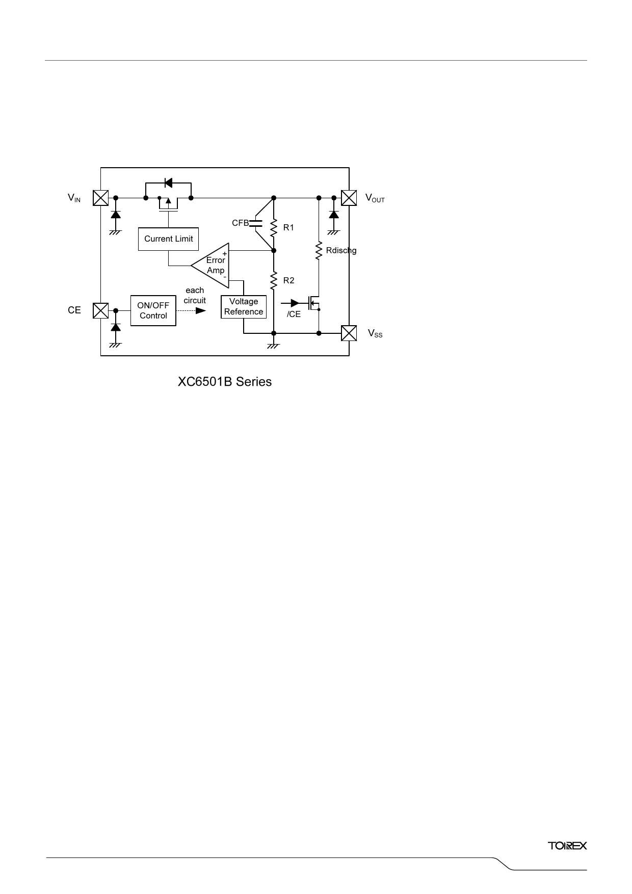
■OPERATIONAL EXPLANATION
The voltage divided by resistors R1 & R2 is compared with the internal reference voltage by the error amplifier. The P-channel
MOSFET which is connected to the VOUT pin is then driven by the subsequent output signal. The output voltage at the VOUT pin
is controlled & stabilized by a system of negative feedback. The current limit circuit and short protect circuit operate in relation
to the level of output current. Further, the IC's internal circuitry can be shutdown via the CE pin's signal.
<CL High Speed Auto-Discharge Function>
The XC6501B/D series can discharge the electric charge in the output capacitor CL, when a low signal to the CE pin, which
enables a whole IC circuit turn off, is inputted via the N-channel transistor located between the VOUT pin and the VSS pin as
shown in the BLOCK DIAGRAM. The CL auto-discharge resistance value is set at 400Ω(VOUT=5.0V @ VIN=6.0V at typical).
The discharge time of the output capacitor CL is set by the CL auto-discharge resistance R and the output capacitor CL. By
setting time constant of a CL auto-discharge resistance value Rdischg and an output capacitor value CL as τ (τ=C x
Rdischg), the output voltage after discharge via the N-channel transistor is calculated by the following formulas.
V = VOUT(E) x e –t/τ, or t=τx In (VOUT(E) / V )
where V : Output voltage after discharge, VOUT(E) : Output voltage, t : Discharge time,
τ: CL auto-discharge resistance Rdischg x Output capacitor CL
<Current Limiter, Short-Circuit Protection>
The XC6501 series’ fold-back circuit operates as an output current limiter and a short protection of the output pin. When the
load current reaches the current limit level, the fixed current limiter circuit operates and output voltage drops. When the
output voltage is shorted to the VSS, its current flow reached and minimized to about 25mA.
<CE Pin>
The IC's internal circuitry can be shutdown via the signal from the CE pin with the XC6501 series. In shutdown mode output at
the VOUT pin will be pulled down to the VSS level via R1 & R2. However, as for the XC6501B/D series, the CL auto-discharge
resistor is connected in parallel to R1 and R2 while the power supply is applied to the VIN pin. Therefore, time until the VOUT pin
reaches the VSS level becomes short. The output voltage becomes unstable, when the CE pin is open. If this IC is used with
the correct output voltage for the CE pin, the logic is fixed and the IC will operate normally. However, supply current may
increase as a result of through current in the IC's internal circuitry when medium voltage is input.
■NOTES ON USE
1. Please use this IC within the stated absolute maximum ratings. The IC is liable to malfunction should the ratings be
exceeded.
2. This IC achieves stable operation without an output capacitor CL by internal phase compensation. However, wiring
impedance is high, operations may become unstable due to noise and/or phase lag depending on output current.
Please wire the input capacitor CIN and the output capacitor CL as close to the IC as possible.
7/21
Share Link: