LC863324B 查看數據表(PDF) - SANYO -> Panasonic
零件编号
产品描述 (功能)
比赛名单
LC863324B Datasheet PDF : 22 Pages
| |||
LC863364B/56B/48B/40B/32B/28B/24B/20B/16B
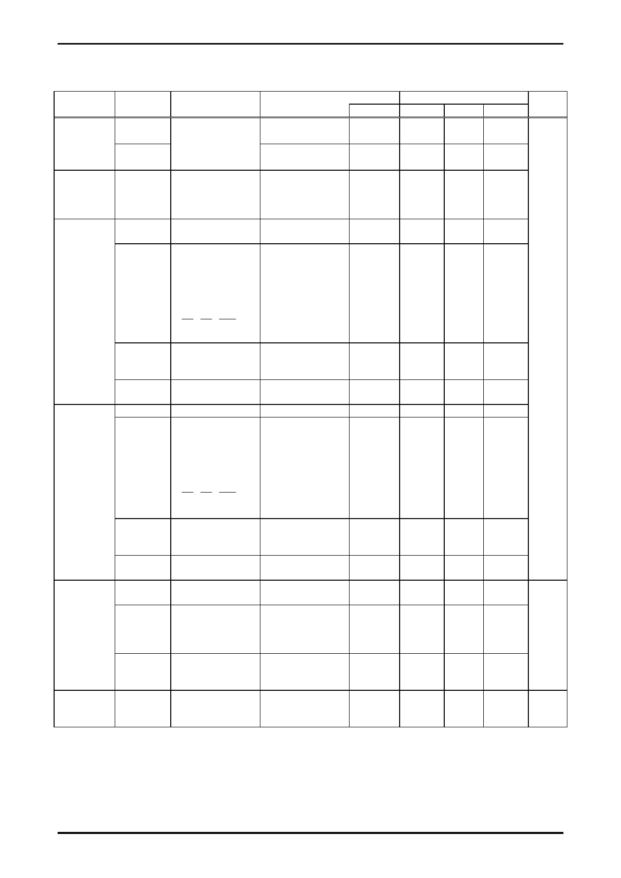
2. Recommended Operating Range at Ta=-10°C to +70°C, VSS=0V
Parameter Symbol
Operating
supply
voltage
range
Hold
voltage
VDD(1)
VDD(2)
VHD
High level VIH(1)
input
voltage
VIH(2)
VIH(3)
VIH(4)
Low level
input
voltage
VIL(1)
VIL(2)
VIL(3)
VIL(4)
Operation tCYC(1)
cycle time
tCYC(2)
tCYC(3)
Oscillation FmRC
frequency
range
Pins
Conditions
Ratings
VDD[V] min. typ. max.
unit
VDD
0.844µs ≤ tCYC
4.5
5.5
V
≤ 0.852µs
4µs ≤ tCYC ≤
4.5
5.5
400µs
VDD
RAMs and the
2.0
5.5
registers data are
kept in HOLD
mode.
Port 0 (Schumitt) Output disable 4.5 - 5.5 0.6VDD
VDD
•Ports 1,6
(Schumitt)
•Port 7
(Schumitt)
port input/
interrupt
• HS , VS , RES
(Schumitt)
Port 70
Watchdog timer
input
•Port 8
port input
Port 0 (Schumitt)
•Ports 1,6
(Schumitt)
•Port 7
(Schumitt)
port input/
interrupt
• HS , VS , RES
(Schumitt)
Port 70
Watchdog timer
input
Port 8
port input
Output disable
Output disable
Output disable
Output disable
Output disable
Output disable
Output disable
•All functions
operating
•AD converter
operating
•OSD is not
operating
•OSD and AD
converter are
not operating
Internal RC
oscillation
4.5 - 5.5 0.75VDD
VDD
4.5 - 5.5 VDD-0.5
4.5 - 5.5 0.7VDD
4.5 - 5.5 VSS
4.5 - 5.5 VSS
VDD
VDD
0.2VDD
0.25VDD
4.5 - 5.5 VSS
0.6VDD
4.5 - 5.5 VSS
0.3VDD
4.5 - 5.5 0.844 0.848 0.852 µs
4.5 - 5.5 0.844
30
4.5 - 5.5 0.844
400
4.5 - 5.5 0.4
0.8
3.0 MHz
11/22
Share Link: 