GS88037BT-XXXV 查看數據表(PDF) - Giga Semiconductor
零件编号
产品描述 (功能)
比赛名单
GS88037BT-XXXV Datasheet PDF : 19 Pages
| |||
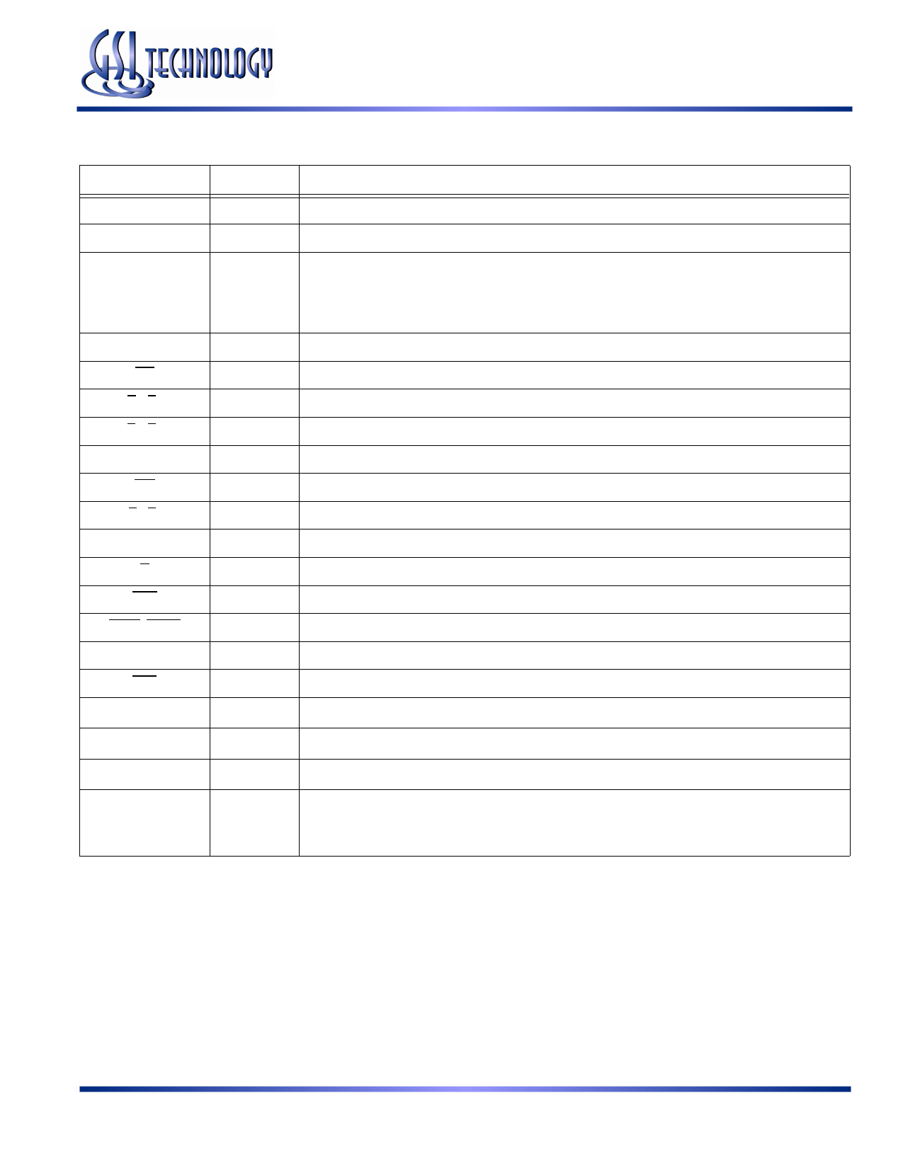
TQFP Pin Description
Symbol
A0, A1
A
DQA
DQB
DQC
DQD
NC
BW
BA, BB
BC, BD
CK
GW
E1, E3
E2
G
ADV
ADSP, ADSC
ZZ
LBO
VDD
VSS
VDDQ
Type
I
I
I/O
—
I
I
I
I
I
I
I
I
I
I
I
I
I
I
I
VDDQ/DNU
—
GS88037BT-xxxV
Description
Address field LSBs and Address Counter preset Inputs
Address Inputs
Data Input and Output pins
No Connect
Byte Write—Writes all enabled bytes; active low
Byte Write Enable for DQA, DQB Data I/Os; active low
Byte Write Enable for DQC, DQD Data I/Os; active low
Clock Input Signal; active high
Global Write Enable—Writes all bytes; active low
Chip Enable; active low
Chip Enable; active high
Output Enable; active low
Burst address counter advance enable; active low
Address Strobe (Processor, Cache Controller); active low
Sleep Mode control; active high
Linear Burst Order mode; active low
Core power supply
I/O and Core Ground
Output driver power supply
VDDQ or VDD (must be tied high)
or
Do Not Use (must be left floating)
Rev: 1.03 6/2006
3/19
Specifications cited are subject to change without notice. For latest documentation see http://www.gsitechnology.com.
© 2002, GSI Technology
Share Link: 