CS8361 查看數據表(PDF) - ON Semiconductor
零件编号
产品描述 (功能)
比赛名单
CS8361 Datasheet PDF : 8 Pages
| |||
CS8361
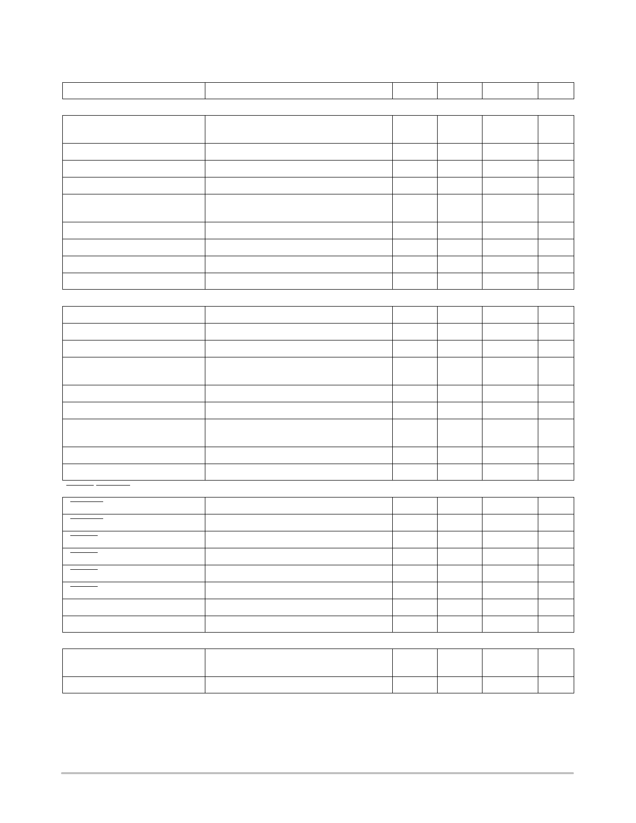
ELECTRICAL CHARACTERISTICS (6.0 V ≤ VIN ≤ 26 V, IOUT1 = IOUT2 = 100 mA, −40°C ≤ TA ≤ +125°C,
−40°C ≤ TJ ≤ +150°C; unless otherwise stated.)
Characteristic
Test Conditions
Min
Typ
Tracking Output (VTRK)
VTRK Tracking Error (VSTBY − VTRK) 6.0 V ≤ VIN ≤ 26 V, 100 mA ≤ ITRK ≤ 250 mA.
−25
−
Note 3
Adjust Pin Current, IAdj
Loop in Regulation
−
1.5
Line Regulation
6.0 V ≤ VIN ≤ 26 V. Note 3
−
5.0
Load Regulation
100 mA ≤ ITRK ≤ 250 mA. Note 3
−
5.0
Dropout Voltage (VIN − VTRK)
ITRK = 100 mA.
ITRK = 250 mA
−
100
−
400
Current Limit
VIN = 12 V, VTRK = 4.5 V
275
500
Quiescent Current
VIN = 12 V, ITRK = 250 mA, No Load on VSTBY
−
25
Reverse Current
VTRK = 5.0 V, VIN = 0 V
−
200
Ripple Rejection
f = 120 Hz, ITRK = 250 mA, 7.0 V ≤ VIN ≤ 17 V
60
70
Standby Output (VSTBY)
Output Voltage, VSTBY
6.0 V ≤ VIN ≤ 26 V, 100 mA ≤ ISTBY ≤ 100 mA.
4.9
5.0
Line Regulation
6.0 V ≤ VIN ≤ 26 V.
−
5.0
Load Regulation
100 mA ≤ ISTBY ≤ 100 mA.
−
5.0
Dropout Voltage (VIN − VSTBY)
ISTBY = 100 mA.
ISTBY = 100 mA
−
100
−
400
Current Limit
VIN = 12 V, VSTBY = 4.5 V
125
200
Short Circuit Current
VIN = 12 V, VSTBY = 0 V
10
100
Quiescent Current
VIN = 12 V, ISTBY = 100 mA, ITRK = 0 mA
VIN = 12 V, ISTBY = 300 mA, ITRK = 0 mA
−
10
−
140
Reverse Current
VSTBY = 5.0 V, VIN = 0 V
−
100
Ripple Rejection
f = 120 Hz, ISTBY = 100 mA, 7.0 V ≤ VIN ≤ 17 V
60
70
RESET ENABLE Functions
ENABLE Input Threshold
−
0.8
1.2
ENABLE Input Bias Current
RESET Threshold High (VRH)
RESET Hysteresis
VENABLE = 0 V to 10 V
VSTBY Increasing
−
−10
0
4.59
4.87
60
120
RESET Threshold Low (VRL)
RESET Leakage
VSTBY Decreasing
−
4.53
4.75
−
−
Output Voltage, Low (VRLO)
1.0 V ≤ VSTBY ≤ VRL, RRST = 10 kW
Output Voltage, Low (VRPEAK)
VSTBY, Power Up, Power Down
Protection Circuitry (Both Outputs)
−
0.1
−
0.6
Independent Thermal Shutdown
VSTBY
VTRK
Overvoltage Shutdown
−
150
180
150
165
30
34
3. VTRK connected to Adj lead. VTRK can be set to higher values by using an external resistor divider.
Max
Unit
+25
mV
5.0
mA
50
mV
50
mV
150
mV
700
mV
−
mA
50
mA
1500
mA
−
dB
5.1
V
50
mV
50
mV
150
mV
600
mV
−
mA
−
mA
20
mA
200
mA
200
mA
−
dB
2.0
V
10
mA
VSTBY − 0.02
V
180
mV
VSTBY − 0.08
V
25
mA
0.4
V
1.0
V
−
°C
−
°C
38
V
http://onsemi.com
3
Share Link: 