SAKC505C-LM 查看數據表(PDF) - Siemens AG
零件编号
产品描述 (功能)
比赛名单
SAKC505C-LM Datasheet PDF : 85 Pages
| |||
C505 / C505C
C505A / C505CA
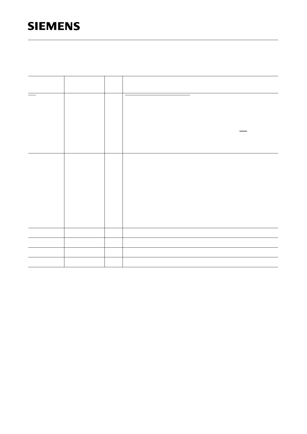
Table 3
Pin Definitions and Functions (cont’d)
Symbol
EA
Pin Number I/O
*)
29
I
P0.0-P0.7 37-30
I/O
VAREF
38
–
VAGND
39
–
VSS
16
–
VCC
17
–
*) I = Input
O = Output
Function
External Access Enable
When held at high level, instructions are fetched from the
internal ROM or OTP memory when the PC is less than
4000H (C505 and C505C) or less than 8000H (C505A and
C505CA). When held at low level, the C505 fetches all
instructions from external program memory. EA should not
be driven during reset operation.
For the C505-L and the C505C-L this pin must be tied low.
Port 0
is an 8-bit open-drain bidirectional I/O port. Port 0 pins that
have 1’s written to them float, and in that state can be used
as high-impendance inputs. Port 0 is also the multiplexed
low-order address and data bus during accesses to external
program or data memory. In this application it uses strong
internal pullup transistors when issuing 1’s.
Port 0 also outputs the code bytes during program
verification in the C505-2R/C505C-2R. External pullup
resistors are required during program verification.
Reference voltage for the A/D converter.
Reference ground for the A/D converter.
Ground (0 V)
Power Supply (+ 5 V)
Semiconductor Group
12
1997-12-01
Share Link: 