SAKC505L 查看數據表(PDF) - Infineon Technologies
零件编号
产品描述 (功能)
比赛名单
SAKC505L Datasheet PDF : 85 Pages
| |||
C505L
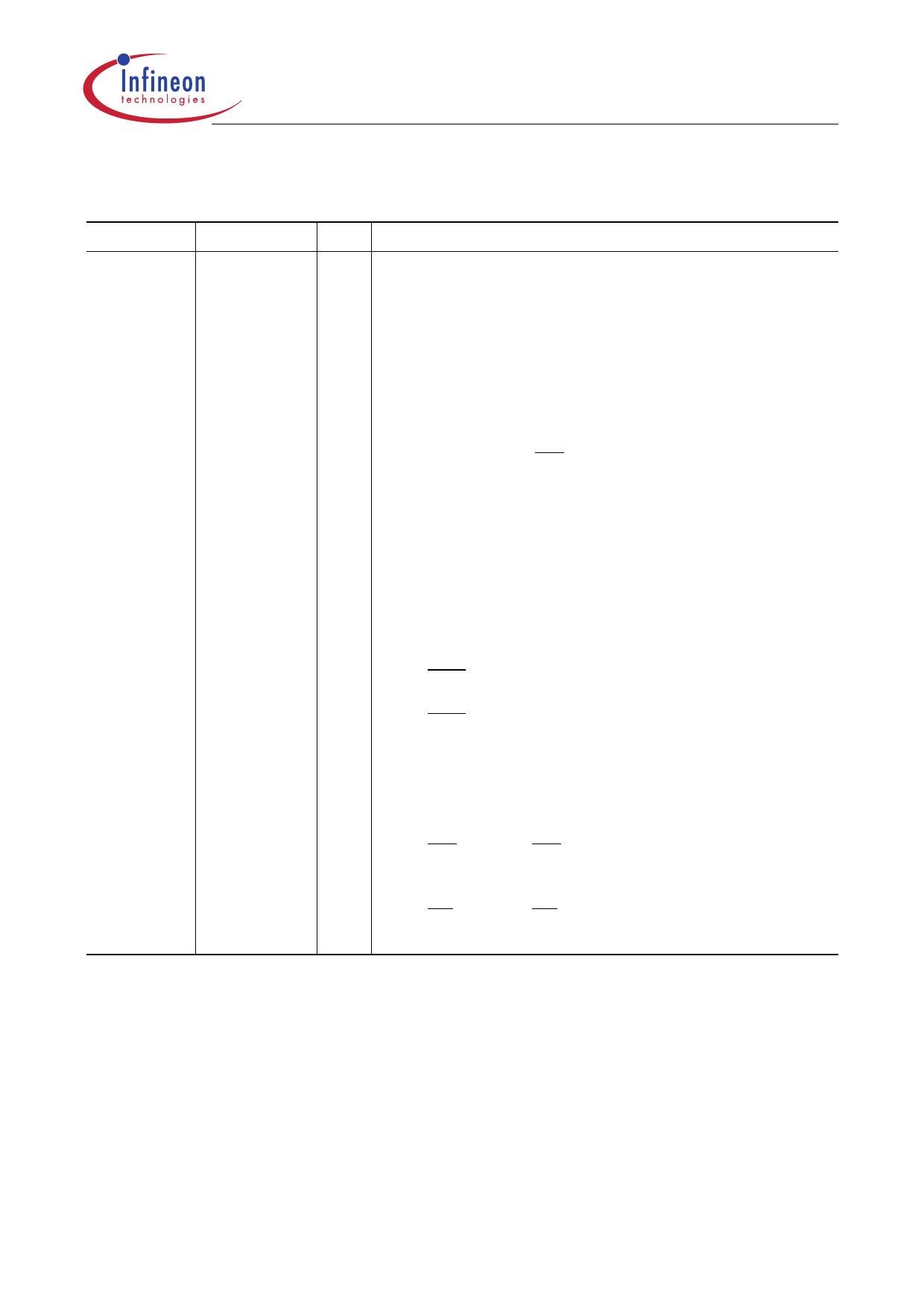
Table 1
Pin Definitions and Functions (cont’d)
Symbol
Pin Number I/O*) Function
P3.7-P3.0 35-42
42
41
40
39
38
37
36
35
I/O Port 3
is an 8-bit quasi-bidirectional port with internal pull-up
arrangement. Port 3 pins that have a 1 written to them are
pulled high by the internal pull-up transistors and in that
state can be used as inputs. As inputs, port 3 pins being
externally pulled low will source current (IIL, in the DC
characteristics) because of the internal pullup transistors.
The output latch corresponding to a secondary function
must be programmed to a one (1) for that function to operate
(except for TxD and WR).
P3.4 and P3.5 can also be configured as LCD column
outputs C31 and C30 respectively. These pins should not be
used for input when configured as LCD output pins.
The secondary functions are assigned to the pins of port 3
as follows:
P3.0 / RxD
Receiver data input (asynch.) or data
input/output (synch.) of serial interface
P3.1 / TxD
Transmitter data output (asynch.) or
clock output (synch.) of serial interface
P3.2 / INT0
External interrupt 0 input / timer 0 gate
control input
P3.3 / INT1
External interrupt 1 input / timer 1 gate
control input
P3.4 / T0 / C31 Timer 0 counter input / LCD column 31
output
P3.5 / T1 / C30 Timer 1 counter input / LCD column 30
output
P3.6 / WR
WR control output; latches the data
byte from port 0 into the external data
memory
P3.7 / RD
RD control output; enables the external
data memory
*) I = Input
O = Output
Data Sheet
7
06.99
Share Link: 