TDA8133 查看數據表(PDF) - STMicroelectronics
零件编号
产品描述 (功能)
比赛名单
TDA8133 Datasheet PDF : 13 Pages
| |||
TDA8133/D
POWER DISSIPATION AND LAYOUT INDICATIONS
5 POWER DISSIPATION AND LAYOUT INDICATIONS
The power is mainly dissipated by the two device buffers. It can be calculated by the equation:
P = (VIN1-VO1) x IO1 + (VIN2-VO2) x IO2
The following table lists the different RthJA values of these packages with or without a heat sink and
the corresponding maximum power dissipation assuming:
q Maximum Ambient Temperature = 70° C
q Maximum Junction Temperature = 140° C
Device
TDA8133
TDA8133D
Heat Sink
No
Yes
No
Yes
RthJA in °C/W
50
20
56 to 40
32
PMAX in W
1.4
3.5
1.25 to 1.75
2.2
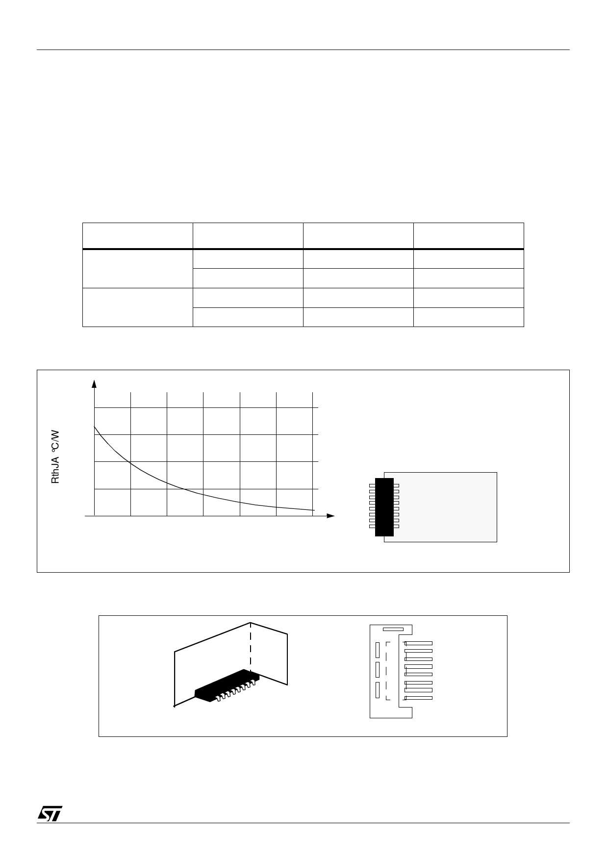
Figure 7: Thermal Resistance (Junction-to-Ambient) of DIP16 Package without Heat Sink
To optimize the thermal conductivity of the copper
60
layer and the exchanges with the air, the solder
must cover the maximum amount of this area.
55
Test Board with
50
“On Board” square heat sink area.
45
40
0
2
4
6
8
10 12
Copper area (cm²) (35 µm plus solder) Board is face-down
Figure 8: Metal plate mounted near the TDA8133D for heat sinking
Top View
Bottom View
9/13
Share Link: 