R3112X 查看數據表(PDF) - RICOH Co.,Ltd.
零件编号
产品描述 (功能)
比赛名单
R3112X Datasheet PDF : 30 Pages
| |||
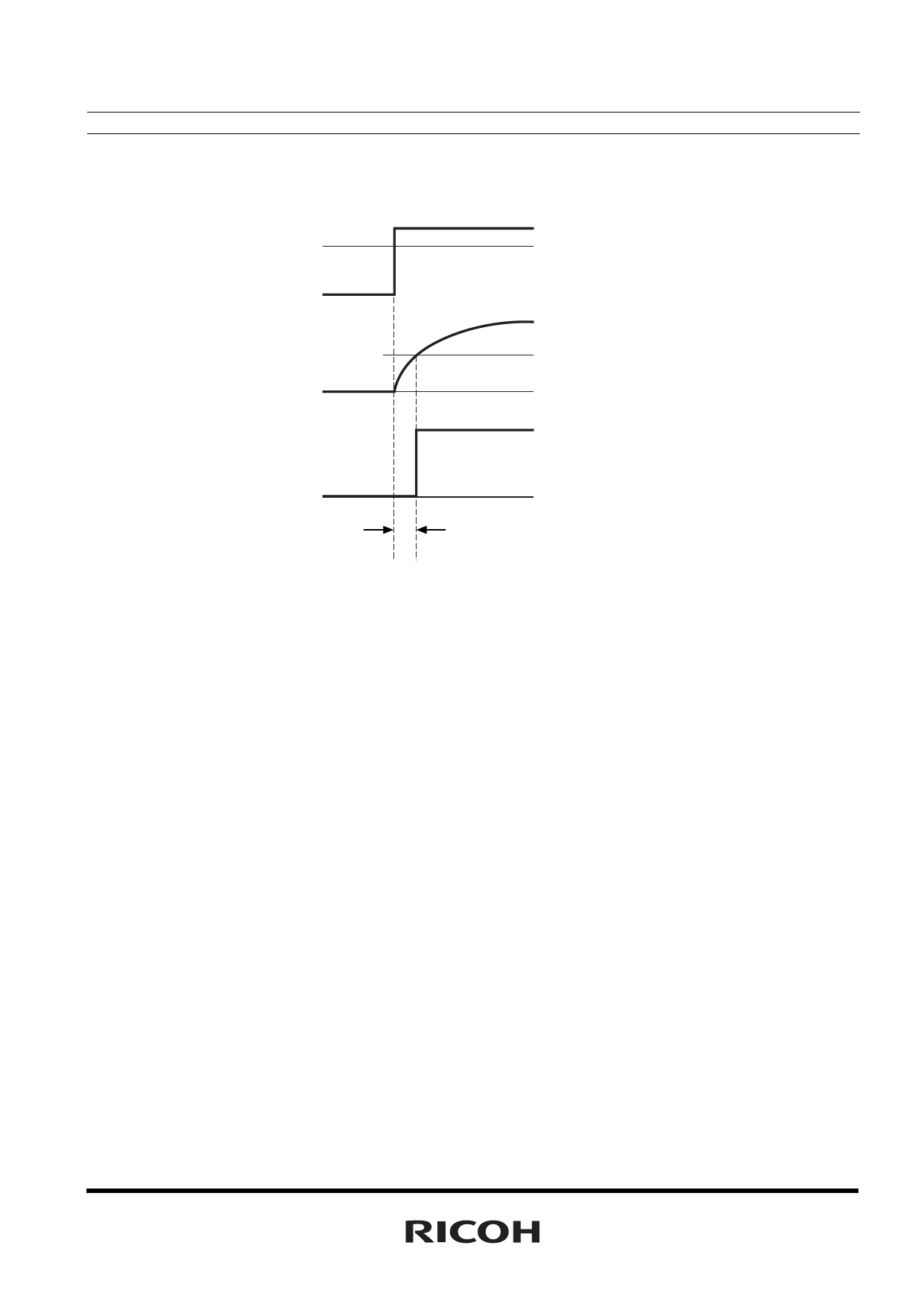
• Operation of Output Delay
Supply Voltage
Released Voltage (+VDET)
R3112x
Capacitor Voltage
CD Pin Threshold Voltage (VTCD)
GND
Output Voltage
GND
Output Delay Time(tD)
When the supply voltage which is higher than released voltage is forced to VDD pin, charge to an external
capacitor starts, then capacitor voltage increases. Until the capacitor voltage reaches to CD Pin threshold voltage,
output voltage maintains “L”. When the capacitor voltage becomes higher than CD pin threshold voltage, output
voltage is reversed from "L” to "H". Where, the time interval between the rising edge of supply voltage and output
voltage reverse point means output delay time.
• Output Delay Time
Output Delay Time (tD) can be calculated with the next formula.
tD=0.69×RD×CD(s)
RD is internal resistor and set at 6.5MΩ(Typ.) typically. CD(F) describes the capacitance value of an external
capacitor. Therefore,
tD=0.69×6.5×106×CD(s)
11
Share Link: 