AS5040(2004) 查看數據表(PDF) - austriamicrosystems AG
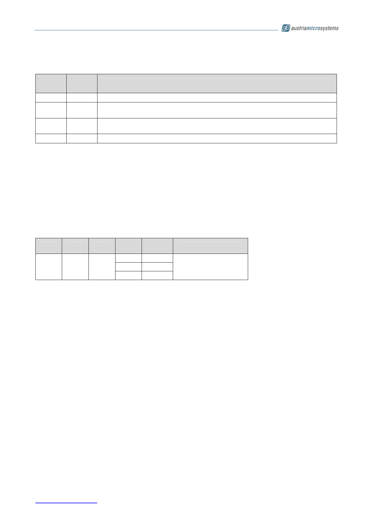
零件编号
产品描述 (功能)
比赛名单
AS5040 Datasheet PDF : 20 Pages
| |||
AS5040 10-BIT PROGRAMMABLE MAGNETIC ROTARY ENCODER
Alignment Mode
The alignment mode simplifies centering the magnet over
the center of the chip to gain maximum accuracy.
Alignment mode can be enabled with the falling edge of
CSn while PROG = logic high (Figure 13). The Data bits
D9-D0 of the SSI change to a 10bit displacement
amplitude output. The magnet is properly aligned, when
the reading is =< 32 at all rotation angles. The larger the
value, the further the magnet is off-center at that
particular angle.
The MagINCn and MagDECn indicators will be = 1 when
the alignment mode reading is > 32. A properly aligned
magnet will produce a MagINCn = MagDECn = 0 signal
throughout a full 360° turn of the magnet.
The Alignment mode can be reset to normal operation
mode by a power-on-reset (disconnect / re-connect
power supply).
5V Operation
100n
VDD5V
VDD3V3
LDO
1...10µF
Internal
VDD
I
4.5 - 5.5V
N
T
E
R
F
A
C
E
VSS
DO
PW M_LSB
CLK
CSn
A_LSB_U
B_Dir_V
Index_W
Prog
PROG
CSn
AlignMode Enable
Read-out
via SSI
2µs 2µs
min. min.
Figure 13: Enabling the alignment mode
3.3V / 5V Operation
The AS5040 operates either at 3.3V ±10% or at 5V
±10%. This is made possible by an internal 3.3V Low-
Dropout (LDO) Voltage regulator. The internal supply
voltage is always taken from the output of the LDO,
meaning that the internal blocks are always operating at
3.3V.
For 3.3V operation, the LDO must be bypassed by
connecting VDD3V3 with VDD5V (see Figure 14).
For 5V operation, the 5V supply is connected to pin
VDD5V, while VDD3V3 (LDO output) must be buffered by
a 1...10µF capacitor, which is supposed to be placed
close to the supply pin (see Figure 14).
The VDD3V3 output is intended for internal use only It
must not be loaded with an external load.
The output voltage of the digital interface I/O’s
corresponds to the voltage at pin VDD5V, as the I/O
buffers are supplied from this pin (see Figure 14).
3.3V Operation
VDD5V
VDD3V3
LDO
3.0 - 3.6V
VSS
Internal
VDD
I
N
T
E
R
F
A
C
E
100n
DO
PW M_LSB
CLK
CSn
A_LSB_U
B_Dir_V
Index_W
Prog
Figure 14: Connections for 5V / 3.3V supply voltages
A buffer capacitor of 100nF is recommended in both
cases close to pin VDD5V.
Revision 1.1
www.austriamicrosystems.com
Page 11 of 20
Share Link: 