MC100E156 查看數據表(PDF) - Motorola => Freescale
零件编号
产品描述 (功能)
比赛名单
MC100E156 Datasheet PDF : 4 Pages
| |||
MOTOROLA
SEMICONDUCTOR TECHNICAL DATA
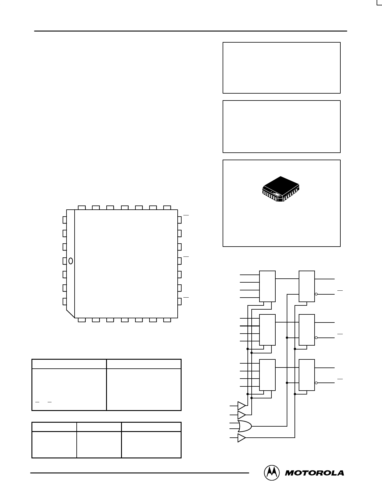
3ĆBit 4:1 MuxĆLatch
The MC10E/100E156 contains three 4:1 multiplexers followed by
transparent latches with differential outputs. When both Latch Enables
(LEN1, LEN2) are LOW, the latch is transparent, and output date is
controlled by the multiplexer select controls (SEL0, SEL1). A logic HIGH
on either LEN1 or LEN2 (or both) latches the outputs. The Master Reset
(MR) overrides all other controls to set the Q outputs LOW.
• 950ps Max. D to Output
• 850ps Max. LEN to Output
• Differential Outputs
• Asynchronous Master Reset
• Dual Latch-Enables
• Extended 100E VEE Range of – 4.2V to – 5.46V
• 75kΩ Input Pulldown Resistors
MC10E156
MC100E156
3-BIT 4:1
MUX-LATCH
Pinout: 28-Lead PLCC (Top View)
D1b D1a D2d D2c D2b D2a VCCO
25 24 23 22 21 20 19
SEL0 26
18 Q2
SEL1 27
17 Q2
FN SUFFIX
PLASTIC PACKAGE
CASE 776-02
MR 28
16 VCC
VEE 1
15 Q1
LOGIC DIAGRAM
LEN1 2
LEN2 3
D1c 4
14 Q1
13 VCCO
12 Q0
D0a
D
D0b
4:1
Q0
D0c
MUX
D0d
EN
R
Q0
5 6 7 8 9 10 11
D1d D0a D0b D0c D0d VCCO Q0
* All VCC and VCCO pins are tied together on the die.
PIN NAMES
Pin
D0x – D3x
SEL0, SEL1
LEN1, LEN2
MR
Q0 – Q2
Q0 – Q2
FUNCTION TABLE
SEL1
L
L
H
H
Function
Input Data
Select Inputs
Latch Enables
Master Reset
True Outputs
Inverted Outputs
SEL0
L
H
L
H
Data
a
b
c
d
D1a
D
D1b
4:1
Q1
D1c
MUX
EN
D1d
R
Q1
D2a
D
D2b
4:1
Q2
D2c
MUX
D2d
EN
R
Q2
SEL0
SEL1
LEN1
LEN2
MR
7/96
© Motorola, Inc. 1996
2–1
REV 3
Share Link: 