MC14070B 查看數據表(PDF) - ON Semiconductor
零件编号
产品描述 (功能)
比赛名单
MC14070B Datasheet PDF : 7 Pages
| |||
MC14070B, MC14077B
CMOS SSI
Quad Exclusive “OR” and “NOR” Gates
The MC14070B quad exclusive OR gate and the MC14077B quad
exclusive NOR gate are constructed with MOS P−channel and
N−channel enhancement mode devices in a single monolithic
structure. These complementary MOS logic gates find primary use
where low power dissipation and/or high noise immunity is desired.
Features
• Supply Voltage Range = 3.0 Vdc to 18 Vdc
• All Outputs Buffered
• Capable of Driving Two Low−Power TTL Loads or One Low−Power
Schottky TTL Load Over the Rated Temperature Range
• Double Diode Protection on All Inputs
• MC14070B − Replacement for CD4030B and CD4070B Types
• MC14077B − Replacement for CD4077B Type
• Pb−Free Packages are Available
MAXIMUM RATINGS (Voltages Referenced to VSS)
Symbol
Parameter
Value
Unit
VDD
Vin, Vout
DC Supply Voltage Range
Input or Output Voltage Range
(DC or Transient)
−0.5 to +18.0
V
−0.5 to VDD + 0.5
V
Iin, Iout
Input or Output Current
(DC or Transient) per Pin
± 10
mA
PD
Power Dissipation, per Package
500
mW
(Note 1)
TA
Ambient Temperature Range
Tstg
Storage Temperature Range
TL
Lead Temperature
(8−Second Soldering)
−55 to +125
°C
−65 to +150
°C
260
°C
Stresses exceeding Maximum Ratings may damage the device. Maximum
Ratings are stress ratings only. Functional operation above the Recommended
Operating Conditions is not implied. Extended exposure to stresses above the
Recommended Operating Conditions may affect device reliability.
1. Temperature Derating:
Plastic “P and D/DW” Packages: – 7.0 mW/_C From 65_C To 125_C
This device contains protection circuitry to guard against damage due to high
static voltages or electric fields. However, precautions must be taken to avoid
applications of any voltage higher than maximum rated voltages to this
high−impedance circuit. For proper operation, Vin and Vout should be constrained
to the range VSS v (Vin or Vout) v VDD.
Unused inputs must always be tied to an appropriate logic voltage level
(e.g., either VSS or VDD). Unused outputs must be left open.
http://onsemi.com
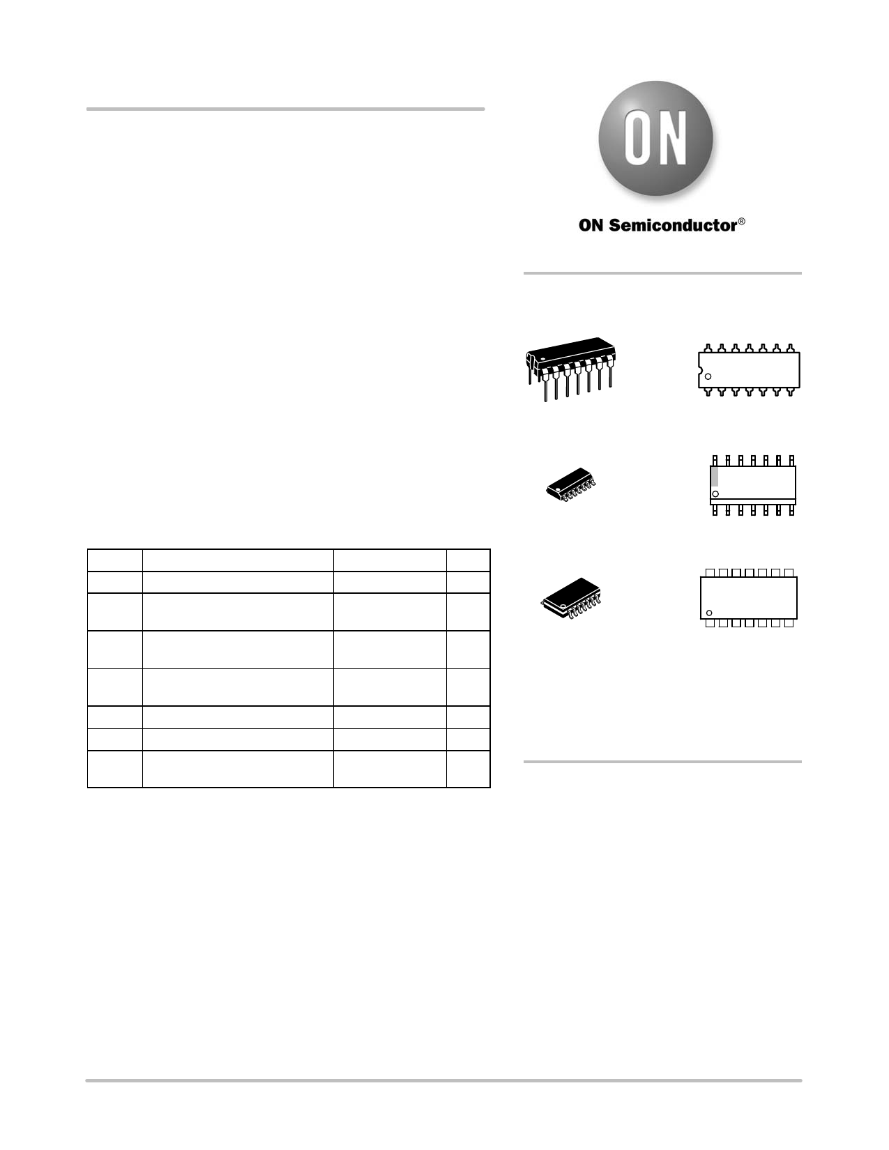
MARKING
DIAGRAMS
PDIP−14
P SUFFIX
CASE 646
14
MC140xxBCP
AWLYYWWG
1
14
SOIC−14
D SUFFIX
CASE 751A
140xxBG
AWLYWW
1
SOEIAJ−14
F SUFFIX
CASE 965
14
MC140xxB
ALYWG
1
xx
A
WL, L
YY, Y
WW, W
G
= Specific Device Code
= Assembly Location
= Wafer Lot
= Year
= Work Week
= Pb−Free Package
ORDERING INFORMATION
See detailed ordering and shipping information in the package
dimensions section on page 3 of this data sheet.
© Semiconductor Components Industries, LLC, 2006
1
October, 2006 − Rev. 7
Publication Order Number:
MC14070B/D
Share Link: 